SLVSFI5A October   2020  – December 2020 TLC6C5748-Q1

PRODUCTION DATA  

  1. Features
  2. Applications
  3. Description
  4. Revision History
  5. Terminal Configurations and Functions
  6. Specifications
    1. 6.1 Absolute Maximum Ratings
    2. 6.2 ESD Ratings
    3. 6.3 Recommended Operating Conditions
    4. 6.4 Thermal Information
    5. 6.5 Electrical Characteristics
    6. 6.6 Switching Characteristics
    7. 6.7 Typical Characteristics
  7. Parameter Measurement Information
    1. 7.1 Terminal-Equivalent Input and Output Schematic Diagrams
    2. 7.2 Test Circuits
    3. 7.3 Timing Diagrams
  8. Detailed Description
    1. 8.1 Overview
    2. 8.2 Functional Block Diagram
    3. 8.3 Feature Description
      1. 8.3.1 Output Current Calculation
      2. 8.3.2 Register and Data Latch Configuration
        1. 8.3.2.1 769-Bit Common Shift Register
        2. 8.3.2.2 Grayscale (GS) Data Latch
        3. 8.3.2.3 Control Data Latch
        4. 8.3.2.4 Dot Correction (DC) Data Latch
        5. 8.3.2.5 Maximum Current (MC) Data Latch
        6. 8.3.2.6 Global Brightness Control (BC) Data Latch
        7. 8.3.2.7 Function Control (FC) Data Latch
      3. 8.3.3 Status Information Data (SID)
      4. 8.3.4 LED Open Detection (LOD)
      5. 8.3.5 LED Short Detection (LSD)
      6. 8.3.6 Thermal Shutdown Faults (TSD)
      7. 8.3.7 Noise Reduction
    4. 8.4 Device Functional Modes
      1. 8.4.1 Maximum Current Control (MC) Function
      2. 8.4.2 Dot Correction (DC) Function
      3. 8.4.3 Global Brightness Control (BC) Function
      4. 8.4.4 Grayscale (GS) Function (PWM Control)
        1. 8.4.4.1 Conventional PWM Control
        2. 8.4.4.2 Enhanced Spectrum (ES) PWM Control
        3. 8.4.4.3 Auto Display Repeat Function
        4. 8.4.4.4 Display Timing Reset Function
        5. 8.4.4.5 Auto Data Refresh Function
  9. Application and Implementation
    1. 9.1 Application Information
    2. 9.2 Typical Application
      1. 9.2.1 Daisy-Chain Application
        1. 9.2.1.1 Design Requirements
        2. 9.2.1.2 Detailed Design Procedure
          1. 9.2.1.2.1 Step-by-Step Design Procedure
          2. 9.2.1.2.2 Maximum Current (MC) Data
          3. 9.2.1.2.3 Global Brightness Control (BC) Data
          4. 9.2.1.2.4 Dot Correction (DC) Data
          5. 9.2.1.2.5 Grayscale (GS) Data
          6. 9.2.1.2.6 Other Control Data
        3. 9.2.1.3 Application Curves
  10. 10Power Supply Recommendations
  11. 11Layout
    1. 11.1 Layout Guidelines
    2. 11.2 Layout Example
  12. 12Device and Documentation Support
    1. 12.1 Receiving Notification of Documentation Updates
    2. 12.2 Support Resources
    3. 12.3 Trademarks
    4. 12.4 Electrostatic Discharge Caution
    5. 12.5 Glossary
  13. 13Mechanical, Packaging, and Orderable Information

パッケージ・オプション

メカニカル・データ(パッケージ|ピン)
サーマルパッド・メカニカル・データ
発注情報

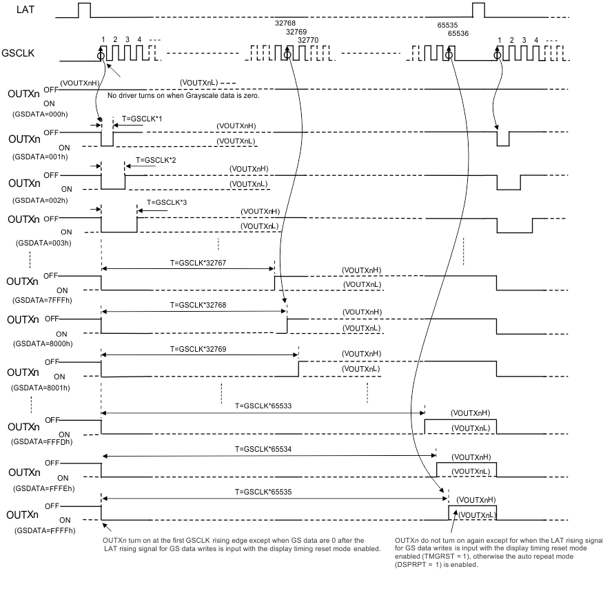
Conventional PWM Control

The first GS clock rising edge increments the GS counter by one and switches on all outputs with a non-zero GS value programmed into the GS data latch. Each additional GS clock rising edge increases the corresponding GS counter by one.

The GS counter keeps track of the number of clock pulses from the respective GS clock inputs. Each output stays on while the counter is less than or equal to the programmed GS value. Each output turns off at the GS counter value rising edge when the counter becomes greater than the output GS latch value. Figure 8-7 illustrates the conventional PWM operation.
GUID-DD061EC2-6F5F-45A2-A941-0D0C11F5120E-low.gifFigure 8-7 Conventional PWM Operation