JAJSP02C march 2011 – april 2023 TLV3011-Q1 , TLV3011B-Q1 , TLV3012-Q1 , TLV3012B-Q1
PRODUCTION DATA
- 1 特長
- 2 アプリケーション
- 3 概要
- 4 Revision History
- 5 Pin Configuration and Functions
-
6 Specifications
- 6.1 Absolute Maximum Ratings TLV3012-Q1 DCK Package Only
- 6.2 Absolute Maximum Ratings - TLV301x-Q1 DBV Package, TLV3011B-Q1 and TLV3012B-Q1
- 6.3 ESD Ratings
- 6.4 Thermal Information - TLV3012-Q1 DCK Package Only
- 6.5 Thermal Information- TLV301x-Q1 DBV Package, TLV3011B-Q1 and TLV3012B-Q1
- 6.6 Recommended Operating Conditions
- 6.7 Electrical Characteristics - TLV3012-Q1 DCK Package Only
- 6.8 Switching Characteristics - TLV3012-Q1 DCK Package Only
- 6.9 Electrical Characteristics- TLV301x-Q1 DBV Package, TLV3011B-Q1 and TLV3012B-Q1
- 6.10 Switching Characteristics- TLV301x-Q1 DBV Package, TLV3011B-Q1 and TLV3012B-Q1
- 7 Typical Characteristics - TLV3012-Q1 DCK Package Only
- 8 Typical Characteristics - TLV301x-Q1 DBV Package, TLV3011B-Q1 and TLV3012B-Q1
- 9 Detailed Description
- 10Application and Implementation
- 11Device and Documentation Support
- 12Mechanical, Packaging, and Orderable Information
パッケージ・オプション
メカニカル・データ(パッケージ|ピン)
サーマルパッド・メカニカル・データ
発注情報
10.3.1 Power-On Reset
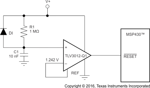
The reset circuit shown in Figure 10-5 provides a time-delayed release of reset to the MSP430™ microcontroller. Operation of the circuit is based on a stabilization time constant of the supply voltage, rather than on a predetermined voltage value. The negative input is a reference voltage created by the internal voltage reference. The positive input is an RC circuit that provides a power-up delay. When power is applied, the output of the comparator is low, holding the processor in the reset condition. Only after allowing time for the supply voltage to stabilize does the positive input of the comparator become higher than the negative input, resulting in a high output state, releasing the processor for operation. The stabilization time required for the supply voltage is adjustable by the selection of the RC component values. Use of a lower-valued resistor in this portion of the circuit does not increase current consumption, because no current flows through the RC circuit after the supply has stabilized.
 Figure 10-5 TLV3012-Q1 Configured as Power-Up Reset Circuit for the MSP430™
Microcontroller
Figure 10-5 TLV3012-Q1 Configured as Power-Up Reset Circuit for the MSP430™
MicrocontrollerThe reset delay needed depends on the power-up characteristics of the system power supply. R1 and C1 are selected to allow enough time for the power supply to stabilize. D1 provides rapid reset if power is lost. In this example, the R1 × C1 time constant is 10 ms.