JAJSJH6E august 2020 – july 2023 TLV3604 , TLV3605 , TLV3607
PRODMIX
- 1
- 1 特長
- 2 アプリケーション
- 3 概要
- 4 Revision History
- 5 Pin Configuration and Functions
- 6 Specifications
- 7 Detailed Description
- 8 Application and Implementation
- 9 Power Supply Recommendations
- 10Layout
- 11Device and Documentation Support
- 12Mechanical, Packaging, and Orderable Information
8.1.3 Latch Functionality
The latch pin for the TLV3605 and TLV3607 holds the output state of the device when the voltage at the LEB/HYST pin is less than 800mV above VEE. This is particularly useful when the output state is intended to remain unchanged. An important consideration of the latch functionality is the latch hold time. Latch hold time is the minimum time (after the latch pin is asserted) required for properly latching the comparator output.
 Figure 8-1 Valid Latch Diagram
Likewise, latch setup time is defined as the time that the input must be stable before the latch pin is asserted low. The figure above illustrates when the input can transition for a valid latch. Note that the typical setup time in the EC table is negative; this is due to the internal trace delays of the LEB/HYST pin relative to the input pin trace delays.
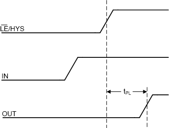
A small delay in the output response is shown below when the TLV3605 and TLV3607 exits a latched output stage.
 Figure 8-2 Latch Disable with Input Change