SNOSDF0 May   2024 TLV4H290-SEP , TLV4H390-SEP

ADVANCE INFORMATION  

  1.   1
  2. Features
  3. Applications
  4. Description
  5. Pin Configuration and Functions
    1. 4.1 Pin Functions:TLV4H290-SEP and TLV4H390-SEP Quad
  6. Specifications
    1. 5.1 Absolute Maximum Ratings
    2. 5.2 ESD Ratings
    3. 5.3 Recommended Operating Conditions
    4. 5.4 Thermal Information, Quad
    5. 5.5 Electrical Characteristics, Quad
    6. 5.6 Switching Characteristics, Quad
    7. 5.7 Typical Characteristics
  7. Detailed Description
    1. 6.1 Overview
    2. 6.2 Functional Block Diagram
    3. 6.3 Feature Description
    4. 6.4 Device Functional Modes
      1. 6.4.1 Outputs
        1. 6.4.1.1 TLV4H290-SEP Open Drain Output
        2. 6.4.1.2 TLV4H390-SEP Push-Pull Output
      2. 6.4.2 Power-On Reset (POR)
      3. 6.4.3 Inputs
        1. 6.4.3.1 Rail to Rail Input
        2. 6.4.3.2 Fault Tolerant Inputs
        3. 6.4.3.3 Input Protection
      4. 6.4.4 ESD Protection
      5. 6.4.5 Unused Inputs
      6. 6.4.6 Hysteresis
  8. Application and Implementation
    1. 7.1 Application Information
      1. 7.1.1 Basic Comparator Definitions
        1. 7.1.1.1 Operation
        2. 7.1.1.2 Propagation Delay
        3. 7.1.1.3 Overdrive Voltage
      2. 7.1.2 Hysteresis
        1. 7.1.2.1 Inverting Comparator With Hysteresis
        2. 7.1.2.2 Non-Inverting Comparator With Hysteresis
        3. 7.1.2.3 Inverting and Non-Inverting Hysteresis using Open-Drain Output
    2. 7.2 Typical Applications
      1. 7.2.1 Window Comparator
        1. 7.2.1.1 Design Requirements
        2. 7.2.1.2 Detailed Design Procedure
        3. 7.2.1.3 Application Curve
      2. 7.2.2 Square-Wave Oscillator
        1. 7.2.2.1 Design Requirements
        2. 7.2.2.2 Detailed Design Procedure
        3. 7.2.2.3 Application Curve
      3. 7.2.3 Adjustable Pulse Width Generator
      4. 7.2.4 Time Delay Generator
      5. 7.2.5 Logic Level Shifter
      6. 7.2.6 One-Shot Multivibrator
      7. 7.2.7 Bi-Stable Multivibrator
      8. 7.2.8 Zero Crossing Detector
      9. 7.2.9 Pulse Slicer
    3. 7.3 Power Supply Recommendations
    4. 7.4 Layout
      1. 7.4.1 Layout Guidelines
      2. 7.4.2 Layout Example
  9. Device and Documentation Support
    1. 8.1 Documentation Support
      1. 8.1.1 Related Documentation
    2. 8.2 Receiving Notification of Documentation Updates
    3. 8.3 Support Resources
    4. 8.4 Trademarks
    5. 8.5 Electrostatic Discharge Caution
    6. 8.6 Glossary
  10. Revision History
  11. 10Mechanical, Packaging, and Orderable Information

パッケージ・オプション

メカニカル・データ(パッケージ|ピン)
サーマルパッド・メカニカル・データ
発注情報

Propagation Delay

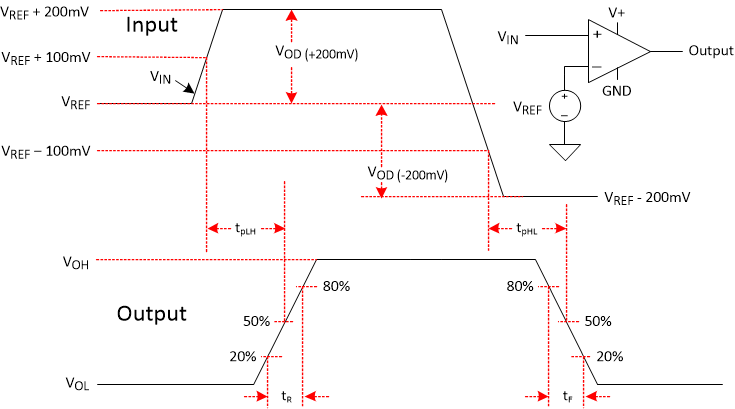
There is a delay between from when the input crosses the reference voltage and the output responds. This is called the Propagation Delay. Propagation delay can be different between high-to low and low-to-high input transitions. This is shown as tpLH and tpHL in Figure 7-1 and is measured from the mid-point of the input to the midpoint of the output.
TLV4H290-SEP TLV4H390-SEP Comparator Timing DiagramFigure 7-1 Comparator Timing Diagram