JAJSDM5E September 2017 – November 2019 TLV7011 , TLV7012 , TLV7021 , TLV7022
PRODUCTION DATA.
- 1 特長
- 2 アプリケーション
- 3 概要
- 4 改訂履歴
- 5 概要 (続き)
- 6 Pin Configuration and Functions
-
7 Specifications
- 7.1 Absolute Maximum Ratings (Single)
- 7.2 Absolute Maximum Ratings (Dual)
- 7.3 ESD Ratings
- 7.4 Recommended Operating Conditions (Single)
- 7.5 Recommended Operating Conditions (Dual)
- 7.6 Thermal Information (Single)
- 7.7 Thermal Information (Dual)
- 7.8 Electrical Characteristics (Single)
- 7.9 Switching Characteristics (Single)
- 7.10 Electrical Characteristics (Dual)
- 7.11 Switching Characteristics (Dual)
- 7.12 Timing Diagrams
- 7.13 Typical Characteristics
- 8 Detailed Description
- 9 Application and Implementation
- 10Power Supply Recommendations
- 11Layout
- 12デバイスおよびドキュメントのサポート
- 13メカニカル、パッケージ、および注文情報
パッケージ・オプション
メカニカル・データ(パッケージ|ピン)
サーマルパッド・メカニカル・データ
- DPW|5
発注情報
8.4.2 Internal Hysteresis
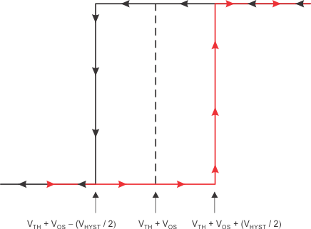
The device hysteresis transfer curve is shown in Figure 37. This curve is a function of three components: VTH, VOS, and VHYST:
- VTH is the actual set voltage or threshold trip voltage.
- VOS is the internal offset voltage between VIN+ and VIN–. This voltage is added to VTH to form the actual trip point at which the comparator must respond to change output states.
- VHYST is the internal hysteresis (or trip window) that is designed to reduce comparator sensitivity to noise
(4.2 mV for the TLV7011).
 Figure 37. Hysteresis Transfer Curve