JAJSDY2J September 2017 – November 2024 TLV7031 , TLV7032 , TLV7034 , TLV7041 , TLV7042 , TLV7044
PRODUCTION DATA
- 1
- 1 特長
- 2 アプリケーション
- 3 概要
- 4 Pin Configuration and Functions
-
5 Specifications
- 5.1 Absolute Maximum Ratings
- 5.2 ESD Ratings
- 5.3 Recommended Operating Conditions
- 5.4 Thermal Information (Single)
- 5.5 Thermal Information (Dual)
- 5.6 Thermal Information (Quad)
- 5.7 Electrical Characteristics (Single)
- 5.8 Switching Characteristics (Single)
- 5.9 Electrical Characteristics (Dual)
- 5.10 Switching Characteristics (Dual)
- 5.11 Electrical Characteristics (Quad)
- 5.12 Switching Characteristics (Quad)
- 5.13 Timing Diagrams
- 5.14 Typical Characteristics
- 6 Detailed Description
- 7 Application and Implementation
- 8 Device and Documentation Support
- 9 Revision History
- 10Mechanical, Packaging, and Orderable Information
パッケージ・オプション
メカニカル・データ(パッケージ|ピン)
サーマルパッド・メカニカル・データ
- DPW|5
発注情報
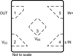
4.1 Pin Functions: TLV7031/41 Singles including "S" and "L" options
 Figure 4-1 Figure 4-1 TLV70x1 "North West" Pinout DBV, DCK, Packages, SOT-23-5, SC-70-5 Top View |  Figure 4-2 Figure 4-2 TLV70x1S "South East" Pinout DBV, DCK Packages, SOT-23-5, SC-70-5 Top View |  Figure 4-3 Figure 4-3 TLV70x1L(2) "TLV/LMC72xx type" Pinout with reversed supplies DBV Package, SOT-23-5 Top View |
 Figure 4-4
 TLV70x1
5-Pin X2SON
Top View
Table 4-1 Pin Functions
| NAME | TLV7031, TLV7041 | TLV7031S, TLV7041S | TLV7031L, TLV7041L(2) | I/O(1) | DESCRIPTION | |
|---|---|---|---|---|---|---|
| PINS | PINS | PINS | ||||
| SOT-23, SC-70 | X2SON(3) | SOT-23, SC-70 | SOT-23 | |||
| OUT | 1 | 1 | 4 | 1 | O | Output |
| V- | 2 | 3 | 2 | 5 | - | Negative Supply Voltage |
| IN+ | 3 | 5 | 1 | 3 | I | Non-Inverting (+) Input |
| IN- | 4 | 4 | 3 | 4 | I | Inverting (-) Input |
| V+ | 5 | 2 | 5 | 2 | - | Positive Supply Voltage |
(1) I = Input, O = Output
(2) The "L" pinout option is provided to replace the LMC72xx and TLV7211 in
legacy designs and is not inteded for new designs. The TLV70x1 or TLV70x1S is recommeded
for new designs.
(3) The application report Designing and Manufacturing With TI's X2SON
Packages (SCEA055) provides more details to optimize PCB designs.