JAJSK01E april   2011  – december 2020 TLV803 , TLV853

PRODUCTION DATA  

  1.   1
  2. 特長
  3. アプリケーション
  4. 概要
  5. Revision History
  6. Device Comparison
  7. Pin Configuration and Functions
    1.     Pin Functions
  8. Specifications
    1. 7.1 Absolute Maximum Ratings #GUID-24157BEB-92B8-46F1-A3B7-B7A06F8BDB0C/SLVSA033153
    2. 7.2 ESD Ratings
    3. 7.3 Thermal Information
    4. 7.4 Recommended Operating Conditions
    5. 7.5 Electrical Characteristics
    6. 7.6 Switching Characteristics
    7. 7.7 Typical Characteristics
  9. Detailed Description
    1. 8.1 Overview
    2. 8.2 Functional Block Diagram
    3. 8.3 Feature Description
      1. 8.3.1 VDD Transient Rejection
      2. 8.3.2 Reset During Power Up and Power Down
      3. 8.3.3 Bidirectional Reset Pins
    4. 8.4 Device Functional Modes
      1. 8.4.1 Normal Operation (VDD > Power-Up Reset Voltage)
      2. 8.4.2 Power On Reset (VDD < Power-Up Reset Voltage)
  10. Application and Implementation
    1. 9.1 Application Information
      1. 9.1.1 Monitoring Multiple Supplies
      2. 9.1.2 Output Level Shifting
    2. 9.2 Typical Application
      1. 9.2.1 Design Requirements
      2. 9.2.2 Detailed Design Procedure
      3. 9.2.3 Application Curves
  11. 10Power Supply Recommendations
  12. 11Layout
    1. 11.1 Layout Guidelines
    2. 11.2 Layout Example
  13. 12Device and Documentation Support
    1. 12.1 Device Support
      1. 12.1.1 Development Support
        1. 12.1.1.1 Evaluation Modules
        2. 12.1.1.2 Spice Models
    2. 12.2 Documentation Support
      1. 12.2.1 Related Documentation
    3. 12.3 Related Links
    4. 12.4 サポート・リソース
    5. 12.5 Trademarks
    6. 12.6 静電気放電に関する注意事項
    7. 12.7 用語集
  14. 13Mechanical, Packaging, and Orderable Information

パッケージ・オプション

メカニカル・データ(パッケージ|ピン)
サーマルパッド・メカニカル・データ
発注情報

Reset During Power Up and Power Down

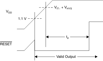
The TLV803 output is valid when VDD is greater than 1.1 V. When VDD is less than 1.1 V, the output transistor turns off and becomes high impedance. The voltage on the RESET pin rises to the voltage level connected to the pull-up resistor. Figure 8-2 shows a typical waveform for power-up, assuming the RESET pin has a pull-up resistor connected to the VDD pin.
GUID-DA2DF579-0CE5-4372-8734-15B9AC91CB2F-low.gifFigure 8-2 Power-Up Response