SLASE75D August 2015 – September 2017 TMDS181
PRODUCTION DATA.
- 1 Features
- 2 Applications
- 3 Description
- 4 Revision History
- 5 Pin Configuration and Functions
-
6 Specifications
- 6.1 Absolute Maximum Ratings
- 6.2 ESD Ratings
- 6.3 Recommended Operating Conditions
- 6.4 Thermal Information
- 6.5 Power Supply Electrical Characteristics
- 6.6 TMDS Differential Input Electrical Characteristics
- 6.7 TMDS Differential Output Electrical Characteristics
- 6.8 DDC, I2C, HPD, and ARC Electrical Characteristics
- 6.9 Power-Up and Operation Timing Requirements
- 6.10 TMDS Switching Characteristics
- 6.11 HPD Switching Characteristics
- 6.12 DDC and I2C Switching Characteristics
- 6.13 Typical Characteristics
- 7 Parameter Measurement Information
-
8 Detailed Description
- 8.1 Overview
- 8.2 Functional Block Diagram
- 8.3
Feature Description
- 8.3.1 Reset Implementation
- 8.3.2 Operation Timing
- 8.3.3 Swap and Polarity Working
- 8.3.4 TMDS Inputs
- 8.3.5 TMDS Inputs Debug Tools
- 8.3.6 Receiver Equalizer
- 8.3.7 Input Signal Detect Block
- 8.3.8 Audio Return Channel
- 8.3.9 Transmitter Impedance Control
- 8.3.10 TMDS Outputs
- 8.3.11 Pre-Emphasis/De-Emphasis
- 8.4 Device Functional Modes
- 8.5 Register Maps
- 9 Application and Implementation
- 10Power Supply Recommendations
- 11Layout
- 12Device and Documentation Support
- 13Mechanical, Packaging, and Orderable Information
パッケージ・オプション
メカニカル・データ(パッケージ|ピン)
- RGZ|48
サーマルパッド・メカニカル・データ
- RGZ|48
発注情報
7 Parameter Measurement Information
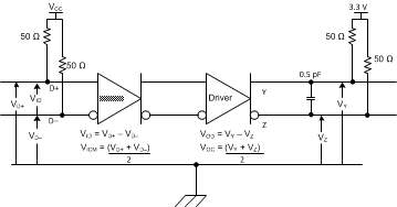 Figure 6. TMDS Main Link Test Circuit
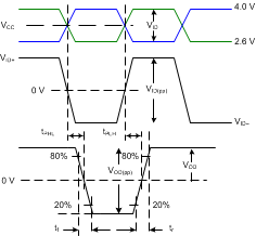 Figure 7. Input/Output Timing Measurements
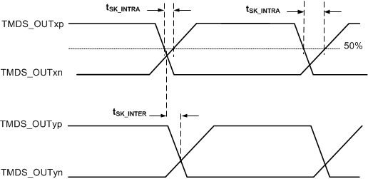 Figure 8. TMDS Output Skew Measurements
 Figure 9. HDMI/DVI TMDS Output Common Mode Measurement
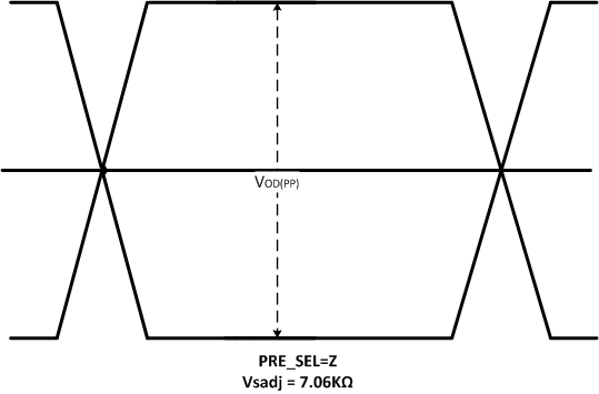 Figure 10. Output Differential Waveform
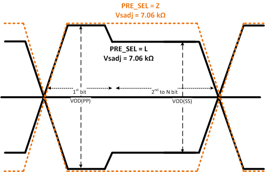 Figure 11. Output De-Emphasis Waveform
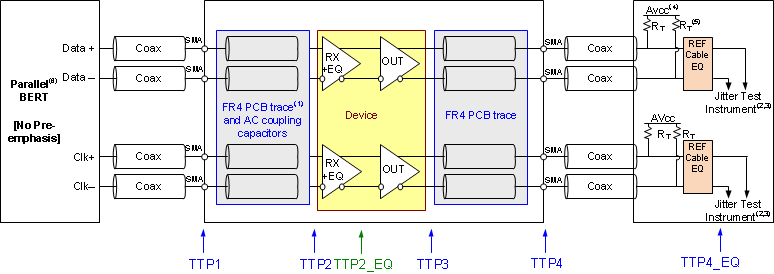
A. The FR4 trace between TTP1 and TTP2 is designed to emulate 1 to 8 inches of FR4, AC coupling capacitor, connector, and another 1 to 8 inches of FR4. Trace width = 4 mils. 100-Ω differential impedance.
B. All jitter is measured at a BER of 10-9
C. Residual jitter reflects the total jitter measured at TTP4 minus the jitter measured at TTP1
D. AVCC = 3.3 V
E. RT = 50 Ω,
F. The input signal from parallel Bert does not have any pre-emphasis. Refer to Recommended Operating Conditions.
Figure 12. HDMI Output Jitter Measurement
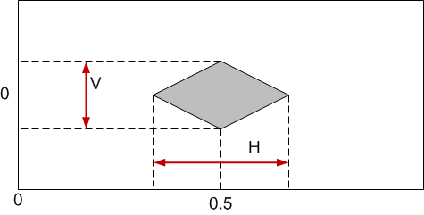
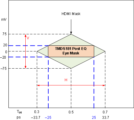 Figure 13. Input Eye Mask Post EQ – TTP2_EQ
Table 1. Output Eye Mask V and H Values
| TMDS Data Rate (Gbps) | H (Tbit) | V (mV) |
|---|---|---|
| 3.4 < DR < 3.712 | 0.6 | 335 |
| 3.712 < DR < 5.94 | –0.0332Rbit2 +0.2312 Rbit + 0.1998 | –19.66Rbit2 + 106.74Rbit + 209.58 |
| 5.94 ≤ DR ≤ 6.0 | 0.4 | 150 |
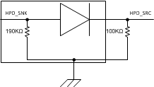 Figure 15. HPD Test Circuit
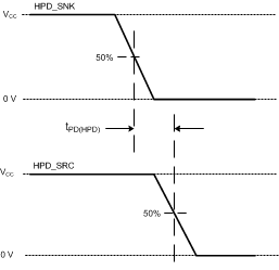 Figure 16. HPD Timing Diagram 1
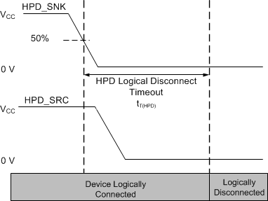 Figure 17. HPD Logic Disconnect Timeout
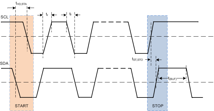 Figure 18. START and STOP Condition Timing
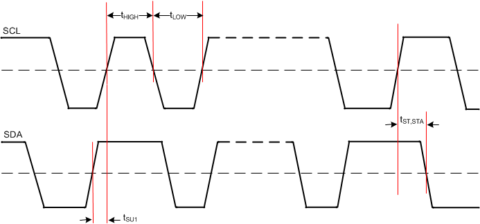 Figure 19. SCL and SDA Timing
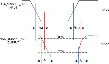 Figure 20. DDC Propagation Delay – Source to Sink
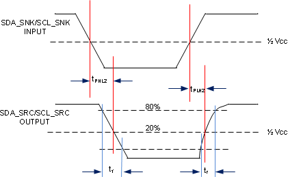 Figure 21. DDC Propagation Delay – Sink to Source
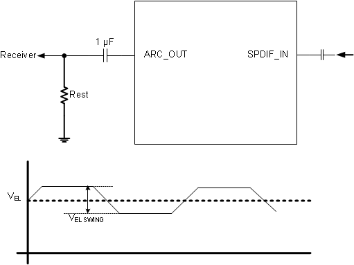 Figure 22. ARC Output
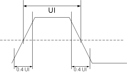 Figure 23. Rise and Fall Time of ARC
