JAJSFY5E August 2018 – December 2019 TMUX6111 , TMUX6112 , TMUX6113
PRODUCTION DATA.
- 1 特長
- 2 アプリケーション
- 3 概要
- 4 改訂履歴
- 5 概要(続き)
- 6 Device Comparison Table
- 7 Pin Configuration and Functions
-
8 Specifications
- 8.1 Absolute Maximum Ratings
- 8.2 ESD Ratings
- 8.3 Thermal Information
- 8.4 Recommended Operating Conditions
- 8.5 Electrical Characteristics (Dual Supplies: ±15 V)
- 8.6 Switching Characteristics (Dual Supplies: ±15 V)
- 8.7 Electrical Characteristics (Single Supply: 12 V)
- 8.8 Switching Characteristics (Single Supply: 12 V)
- 8.9 Typical Characteristics
- 9 Parameter Measurement Information
- 10Detailed Description
- 11Application and Implementation
- 12Power Supply Recommendations
- 13Layout
- 14デバイスおよびドキュメントのサポート
- 15メカニカル、パッケージ、および注文情報
パッケージ・オプション
メカニカル・データ(パッケージ|ピン)
サーマルパッド・メカニカル・データ
- RTE|16
発注情報
10.3.2 Ultra-low Charge Injection
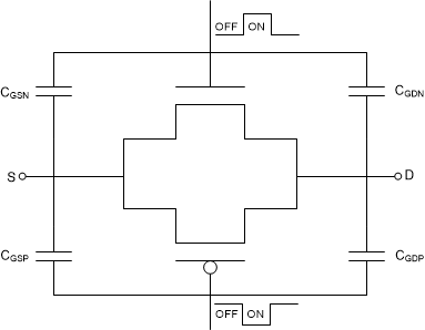
The TMUX6111, TMUX6112, and TMUX6113 are implemented with simple transmission gate topology, as shown in Figure 28. Any mismatch in the stray capacitance associated with the NMOS and PMOS causes an output level change whenever the switch is opened or closed. The devices utilize special charge-injection cancellation circuitry that reduces the source (Sx)-to-drain (Dx) charge injection to as low as 0.6 pC at VS = 0 V, as shown in Figure 29.
 Figure 28. Transmission Gate Topology
  Figure 29. Source-to-Drain Charge Injection vs Source or Drain Voltage