JAJSFY5E August 2018 – December 2019 TMUX6111 , TMUX6112 , TMUX6113
PRODUCTION DATA.
- 1 特長
- 2 アプリケーション
- 3 概要
- 4 改訂履歴
- 5 概要(続き)
- 6 Device Comparison Table
- 7 Pin Configuration and Functions
-
8 Specifications
- 8.1 Absolute Maximum Ratings
- 8.2 ESD Ratings
- 8.3 Thermal Information
- 8.4 Recommended Operating Conditions
- 8.5 Electrical Characteristics (Dual Supplies: ±15 V)
- 8.6 Switching Characteristics (Dual Supplies: ±15 V)
- 8.7 Electrical Characteristics (Single Supply: 12 V)
- 8.8 Switching Characteristics (Single Supply: 12 V)
- 8.9 Typical Characteristics
- 9 Parameter Measurement Information
- 10Detailed Description
- 11Application and Implementation
- 12Power Supply Recommendations
- 13Layout
- 14デバイスおよびドキュメントのサポート
- 15メカニカル、パッケージ、および注文情報
パッケージ・オプション
メカニカル・データ(パッケージ|ピン)
サーマルパッド・メカニカル・データ
- RTE|16
発注情報
12 Power Supply Recommendations
The TMUX6111, TMUX6112, and TMUX6113 operate across a wide supply range of ±5 V to ±17 V (10 V to 17 V in single-supply mode). They also perform well with asymmetrical supplies such as VDD = 12 V and VSS= –5 V. For improved supply noise immunity, use a supply decoupling capacitor ranging from 0.1 µF to 10 µF at both the VDD and VSS pins to ground. Always ensure the ground (GND) connection is established before supplies are ramped. As a best practice, it is recommended to ramp VSS first before VDD in dual or asymmetrical supply applications.
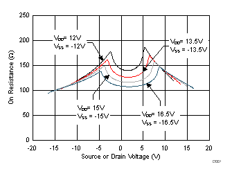
The on-resistance of the devices varies with supply voltage, as illustrated in Figure 32
 Figure 32. On-Resistance Variation With Supply and Input Voltage