JAJSKR5D October 2020 – July 2024 TMUX7211 , TMUX7212 , TMUX7213
PRODUCTION DATA
- 1
- 1 特長
- 2 アプリケーション
- 3 概要
- 4 Device Comparison Table
- 5 Pin Configuration and Functions
-
6 Specifications
- 6.1 Absolute Maximum Ratings
- 6.2 ESD Ratings
- 6.3 Thermal Information
- 6.4 Recommended Operating Conditions
- 6.5 Source or Drain Continuous Current
- 6.6 ±15 V Dual Supply: Electrical Characteristics
- 6.7 ±15 V Dual Supply: Switching Characteristics
- 6.8 ±20 V Dual Supply: Electrical Characteristics
- 6.9 ±20 V Dual Supply: Switching Characteristics
- 6.10 44 V Single Supply: Electrical Characteristics
- 6.11 44 V Single Supply: Switching Characteristics
- 6.12 12 V Single Supply: Electrical Characteristics
- 6.13 12 V Single Supply: Switching Characteristics
- 6.14 Typical Characteristics
- 7 Parameter Measurement Information
- 8 Detailed Description
- 9 Application and Implementation
- 10Device and Documentation Support
- 11Revision History
- 12Mechanical, Packaging, and Orderable Information
パッケージ・オプション
メカニカル・データ(パッケージ|ピン)
サーマルパッド・メカニカル・データ
- RUM|16
発注情報
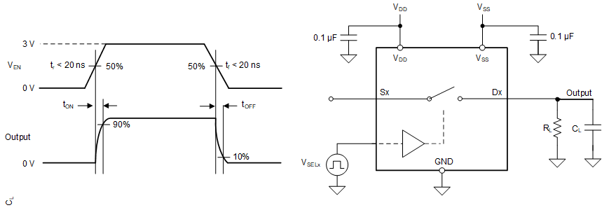
7.4 tON and tOFF Time
Turn-on time is defined as the time taken by the output of the device to rise to 90% after the enable has risen past the logic threshold. The 90% measurement is utilized to provide the timing of the device. System level timing can then account for the time constant added from the load resistance and load capacitance. Figure 7-4 shows the setup used to measure turn-on time, denoted by the symbol tON.
Turn-off time is defined as the time taken by the output of the device to fall to 10% after the enable has fallen past the logic threshold. The 10% measurement is utilized to provide the timing of the device. System level timing can then account for the time constant added from the load resistance and load capacitance. Figure 7-4 shows the setup used to measure turn-off time, denoted by the symbol tOFF.
 Figure 7-4 Turn-On
and Turn-Off Time Measurement Setup