JAJSKR5D October 2020 – July 2024 TMUX7211 , TMUX7212 , TMUX7213
PRODUCTION DATA
- 1
- 1 特長
- 2 アプリケーション
- 3 概要
- 4 Device Comparison Table
- 5 Pin Configuration and Functions
-
6 Specifications
- 6.1 Absolute Maximum Ratings
- 6.2 ESD Ratings
- 6.3 Thermal Information
- 6.4 Recommended Operating Conditions
- 6.5 Source or Drain Continuous Current
- 6.6 ±15 V Dual Supply: Electrical Characteristics
- 6.7 ±15 V Dual Supply: Switching Characteristics
- 6.8 ±20 V Dual Supply: Electrical Characteristics
- 6.9 ±20 V Dual Supply: Switching Characteristics
- 6.10 44 V Single Supply: Electrical Characteristics
- 6.11 44 V Single Supply: Switching Characteristics
- 6.12 12 V Single Supply: Electrical Characteristics
- 6.13 12 V Single Supply: Switching Characteristics
- 6.14 Typical Characteristics
- 7 Parameter Measurement Information
- 8 Detailed Description
- 9 Application and Implementation
- 10Device and Documentation Support
- 11Revision History
- 12Mechanical, Packaging, and Orderable Information
パッケージ・オプション
メカニカル・データ(パッケージ|ピン)
サーマルパッド・メカニカル・データ
- RUM|16
発注情報
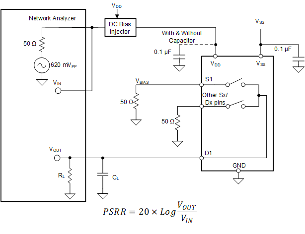
7.12 Power Supply Rejection Ratio (PSRR)
PSRR measures the ability of a device to prevent noise and spurious signals that appear on the supply voltage pin from coupling to the output of the switch. The DC voltage on the device supply is modulated by a sine wave of 100 mVPP. The ratio of the amplitude of signal on the output to the amplitude of the modulated signal is the AC PSRR.
 Figure 7-12 AC PSRR
Measurement Setup