-
TPS20xxC, TPS20xxC-2 Dual Channel, Current-Limited, Power-Distribution Switches SLVSAX6H October 2011 – December 2015 TPS2002C , TPS2003C , TPS2052C , TPS2060C , TPS2062C , TPS2062C-2 , TPS2064C , TPS2064C-2 , TPS2066C , TPS2066C-2
PRODUCTION DATA.
-
TPS20xxC, TPS20xxC-2 Dual Channel, Current-Limited, Power-Distribution Switches
- 1 Features
- 2 Applications
- 3 Description
- 4 Revision History
- 5 Device Comparison Table
- 6 Pin Configuration and Functions
- 7 Specifications
- 8 Parameter Measurement Information
- 9 Detailed Description
- 10Application and Implementation
- 11Power Supply Recommendations
- 12Layout
- 13Device and Documentation Support
- 14Mechanical, Packaging, and Orderable Information
- IMPORTANT NOTICE
TPS20xxC, TPS20xxC-2 Dual Channel, Current-Limited, Power-Distribution Switches
1 Features
- Dual Power Switch Family
- Rated Currents of 0.5 A, 1 A, 1.5 A, 2 A
- Accurate ±20% Current Limit Tolerance
- Fast Overcurrent Response – 2 µs (Typical)
- 70-mΩ (Typical) High-Side N-Channel MOSFET
- Operating Range: 4.5 V to 5.5 V
- Deglitched Fault Reporting (FLTx)
- Selected Parts With (TPS20xxC) and Without (TPS20xxC-2) Output Discharge
- Reverse Current Blocking
- Built-in Softstart
- Pin for Pin With Existing TI Switch Portfolio
- Ambient Temperature Range: –40°C to 85°C
2 Applications
- USB Ports or Hubs, Laptops, Desktops
- High-Definition Digital TVs
- Set Top Boxes
- Short Circuit Protection
3 Description
The TPS20xxC and TPS20xxC-2 dual power-distribution switch family is intended for applications such as USB where heavy capacitive loads and short-circuits may be encountered. This family offers multiple devices with fixed current-limit thresholds for applications between 0.5 A and 2 A.
The TPS20xxC and TPS20xxC-2 dual family limits the output current to a safe level by operating in a constant-current mode when the output load exceeds the current-limit threshold. This provides a predictable fault current under all conditions. The fast overcurrent response time eases the burden on the main 5 V supply to provide regulated power when the output is shorted. The power-switch rise and fall times are controlled to minimize current surges during turnon and turnoff.
Device Information(1)
| PART NUMBER | PACKAGE | BODY SIZE (NOM) |
|---|---|---|
| TPS2052C TPS2062C TPS2066C TPS2066C-2 TPS2060C TPS2064C TPS2064C-2 |
MSOP (8) | 3.00 mm × 3.00 mm |
| TPS2062C TPS2066C |
SOIC (8) | 3.90 mm × 4.90 mm |
| TPS2062C-2 | SON (8) | 3.00 mm × 3.00 mm |
| TPS2002C TPS2003C |
VSON (10) | 3.00 mm × 3.00 mm |
- For all available packages, see the orderable addendum at the end of the data sheet.
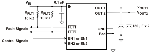
Typical Application
4 Revision History
Changes from G Revision (January 2013) to H Revision
- Added ESD Ratings table, Feature Description section, Device Functional Modes, Application and Implementation section, Power Supply Recommendations section, Layout section, Device and Documentation Support section, and Mechanical, Packaging, and Orderable Information section Go
Changes from F Revision (November 2012) to G Revision
- Changed device TPS2062C-2 SON-8 packages From: Preview To: Active.Go
- Changed devices TPS2066C-2, and TPS2064C-2 MSOP-8 package From: Preview To: ActiveGo
Changes from E Revision (August 2012) to F Revision
- Changed Feature from: Rated Currents of 1 A, 1.5 A, 2 A to: Rated Currents of 0.5 A, 1 A, 1.5 A, 2 AGo
- Changed Feature from: Output Discharge When Disabled to: Selected parts with (TPS20xxC) and without (TPS20xxC-2) Output DischargeGo
- Added TPS2052C, TPS2062C-2, TPS2064C-2, and TPS2066C-2 devices to Table 1Go
- Added TPS2052C, TPS2062C-2, TPS2064C-2, and TPS2066C-2 devices to Table 2Go
- Added TPS2052C, TPS2062C-2, TPS2064C-2, and TPS2066C-2 devices to RECOMMENDED OPERATING CONDITIONS tableGo
- Added TPS2052C and TPS2066C-2 devices to rDS(on)Go
- Added the TPS2052C and TPS2064C-2 devices to IOSGo
- Added Leakage current to Electrical Characteristics tableGo
- Added text to the SOFTSTART, REVERSE BLOCKING AND DISCHARGE OUTPUT sectionGo
- Added last paragraph in the DISCHARGE OUTPUT sectionGo
Changes from D Revision (July 2012) to E Revision
- Changed devices TPS2002C and TPS2003C SON-10 package From: Preview To: ActiveGo
- Changed the IOS current limit values for TPS2002C and 03C (2 A)Go
- Corrected Note 2 reference in the Electrical Characteristics tableGo
Changes from C Revision (June 2012) to D Revision
- Changed the Device Information table, Package Devices and Marking columnsGo
Changes from B Revision (March 2012) to C Revision
- Changed devices TPS2062C and TPS2066C SOIC-8 package From: Preview To: ActiveGo
- Changed the TPS2062C and 66C rDS(on) D package TYP value From: 84 to 90 mΩGo
Changes from A Revision (March 2012) to B Revision
- Changed device TPS2060C MSOP-8 package From: Preview To: ActiveGo
Changes from * Revision (October 2011) to A Revision
5 Device Comparison Table
Table 1. Devices
| DEVICES | RATED CURRENT | STATUS | |||
|---|---|---|---|---|---|
| MSOP-8 (PowerPad™) | SOIC-8 | SON-8 | VSON-10 | ||
| TPS2052C | 0.5 A | Active | — | — | — |
| TPS2062C TPS2066C |
1 A | Active and Active | Active and Active | — | — |
| TPS2062C-2 TPS2066C-2 |
1 A | — and Active | — | Active and — | — |
| TPS2060C TPS2064C |
1.5 A | Active and Active | — | — | — |
| TPS2064C-2 | 1.5 A | Active | — | — | — |
| TPS2002C TPS2003C |
2 A | — | — | — | Active and Active |
6 Pin Configuration and Functions


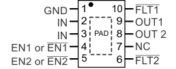

Pin Functions
| PIN | TYPE(3) | DESCRIPTION | ||||
|---|---|---|---|---|---|---|
| NAME | MSOP | SOIC | VSON | SON | ||
| GND | 1 | 1 | 1 | 1 | GND | Ground connection |
| IN | 2 | 2 | 2, 3 | 2 | I | Input voltage and power-switch drain; connect a 0.1 µF or greater ceramic capacitor from IN to GND close to the IC |
| EN1 | 3(1) | 3(6) | 4(4) | — | I | Enable input channel 1, logic high turns on power switch |
| –(2) | –(7) | –(5) | — | |||
| EN1 | –(1) | –(6) | –(4) | 3 | I | Enable input channel 1, logic low turns on power switch |
| 3(2) | 3(7) | 4(5) | ||||
| EN2 | 4(1) | 4(6) | 5(4) | — | I | Enable input channel 2, logic high turns on power switch |
| –(2) | –(7) | –(5) | — | |||
| EN2 | –(1) | –(6) | –(4) | 4 | I | Enable input channel 2, logic low turns on power switch |
| 4(2) | 4(7) | 5(5) | ||||
| FLT2 | 5 | 5 | 6 | 5 | O | Active-low open-drain output, asserted during overcurrent, or overtemperature conditions on channel 2 |
| NC | — | — | 7 | — | O | No connect – leave floating |
| OUT2 | 6 | 6 | 8 | 6 | O | Power-switch output channel 2, connected to load |
| OUT1 | 7 | 7 | 9 | 7 | O | Power-switch output channel 1, connected to load |
| FLT1 | 8 | 8 | 10 | 8 | O | Active-low open-drain output, asserted during over-current, or overtemperature conditions on channel 1 |
| PowerPAD™ | PAD | — | PAD | — | GND | Internally connected to GND; used to heat-sink the part to the circuit board traces. Connect PAD to GND plane as a heatsink. |
7 Specifications
7.1 Absolute Maximum Ratings
over operating free-air temperature range (unless otherwise noted)(1)(2)(3)| MIN | MAX | UNIT | ||
|---|---|---|---|---|
| Voltage range on IN, OUTx, ENx or ENx, FLTx(4) | –0.3 | 6 | V | |
| Voltage range from IN to OUT | –6 | 6 | V | |
| Maximum junction temperature, TJ | Internally limited | °C | ||
| Storage temperature, Tstg | –65 | 150 | °C | |
7.2 ESD Ratings
| VALUE | UNIT | |||
|---|---|---|---|---|
| V(ESD) | Electrostatic discharge | Human-body model (HBM), per ANSI/ESDA/JEDEC JS-001(1) | ±2000 | V |
| Charged-device model (CDM), per JEDEC specification JESD22-C101(2) | ±500 | |||
| IEC 61000-4-2, contact discharge(3) | ±8000 | V | ||
| IEC 61000-4-2, air-gap discharge(3) | ±15000 | |||
7.3 Recommended Operating Conditions
over operating free-air temperature range (unless otherwise noted)| MIN | NOM | MAX | UNIT | |||
|---|---|---|---|---|---|---|
| VIN | Input voltage, IN | 4.5 | 5.5 | V | ||
| VEnable | Input voltage, ENx or ENx | 0 | 5.5 | |||
| IOUTx | Continuous output current, OUTx | TPS2052C | 0.5 | A | ||
| TPS2062C, TPS2062C-2, TPS2066C, and TPS2066C-2 |
1 | |||||
| TPS2060C, TPS2064C, and TPS2064C-2 | 1.5 | |||||
| TPS2002C and TPS2003C | 2 | |||||
| TJ | Operating junction temperature | –40 | 125 | °C | ||
| IFLTx | Sink current into FLTx | 0 | 5 | mA | ||
7.4 Thermal Information
| THERMAL METRIC(1)(2) | TPS2052C TPS2062C TPS2066C TPS2066C-2 TPS2060C TPS2064C TPS2064C-2 |
TPS2062C TPS2066C |
TPS2062C-2 | TPS2002C TPS2003C |
UNIT | |
|---|---|---|---|---|---|---|
| DGN (MSOP) | D (SOIC) | DRB (SON) | DRC (VSON) | |||
| 8 PINS | 8 PINS | 8 PINS | 10 PINS | |||
| RθJA | Junction-to-ambient thermal resistance | 57.2 | 129.9 | 50.8 | 45.4 | °C/W |
| RθJC(top) | Junction-to-case (top) thermal resistance | 110.5 | 83.5 | 60.3 | 58 | °C/W |
| RθJB | Junction-to-board thermal resistance | 60.7 | 70.4 | 26.3 | 21.1 | °C/W |
| ψJT | Junction-to-top characterization parameter | 7.8 | 36.6 | 2.1 | 1.9 | °C/W |
| ψJB | Junction-to-board characterization parameter | 24 | 66.9 | 26.5 | 21.3 | °C/W |
| RθJC(bot) | Junction-to-case (bottom) thermal resistance | 14.3 | n/a | 9.8 | 9.1 | °C/W |
7.5 Electrical Characteristics: TJ = TA = 25°C
VIN = 5 V, VENx = VIN or VENx = 0 V (unless otherwise noted)| PARAMETER | TEST CONDITIONS(1) | MIN | TYP | MAX | UNIT | ||
|---|---|---|---|---|---|---|---|
| POWER SWITCH | |||||||
| rDS(on) | On-resistance | TPS2052C (0.5 A) | DGN | 70 | 84 | mΩ | |
| TPS2052C (0.5 A) –40°C ≤ (TJ, TA) ≤ 85°C |
DGN | 70 | 95 | ||||
| TPS2062C, 66C, and 66C-2 (1 A) | DGN | 70 | 84 | ||||
| TPS2062C, 66C, and 66C-2 (1 A), –40°C ≤ (TJ, TA) ≤ 85°C |
DGN | 70 | 95 | ||||
| TPS2062C and 66C (1 A) | D | 90 | 108 | ||||
| TPS2062C and 66C (1 A) –40°C ≤ (TJ, TA) ≤ 85°C |
D | 90 | 122 | ||||
| TPS2062C-2 (1 A) | DRB | 73 | 87 | ||||
| TPS2062C-2 (1 A) –40°C ≤ (TJ, TA) ≤ 85°C |
DRB | 73 | 101 | ||||
| TPS2060C, 64C, and 64C-2 (1.5 A) | 70 | 84 | |||||
| TPS2060C, 64C, and 64C-2 (1.5 A) –40°C ≤ (TJ, TA) ≤ 85°C |
70 | 95 | |||||
| TPS2002C and 03C (2 A) | 70 | 84 | |||||
| TPS2002C and 03C (2 A) –40°C ≤ (TJ, TA) ≤ 85°C |
70 | 95 | |||||
| CURRENT LIMIT | |||||||
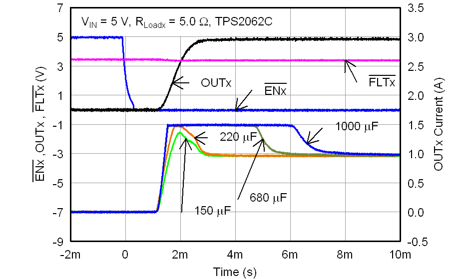
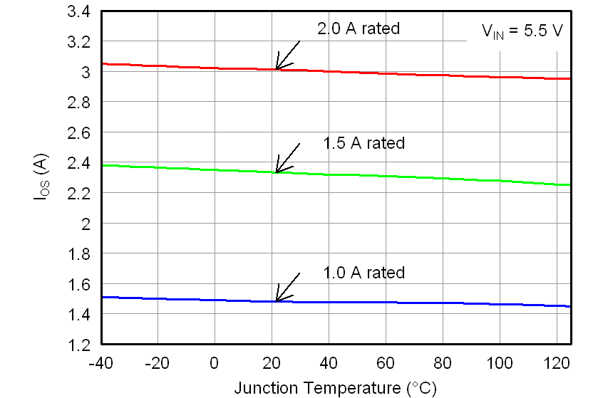
| IOS | Current-limit (see Figure 28) | TPS2052C (0.5 A) | 0.75 | 1 | 1.25 | A | |
| TPS2062C, 62C-2, 66C, and 66C-2 (1 A) | 1.28 | 1.61 | 1.94 | ||||
| TPS2060C, 64C, and 64C-2 (1.5 A) | 1.83 | 2.29 | 2.75 | ||||
| TPS2002C and 03C (2 A) | 2.55 | 3.15 | 3.77 | ||||
| SUPPLY CURRENT | |||||||
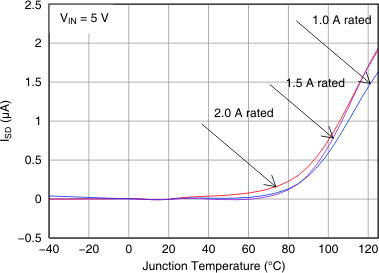
| ISD | Supply current, switch disabled | I(OUTx) = 0 mA | 0.01 | 1 | µA | ||
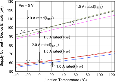
| IS1E | Supply current, single switch enabled | I(OUTx) = 0 mA | 60 | 75 | |||
| IS2E | Supply current, both switches enabled | I(OUTx) = 0 mA | 100 | 120 | |||
| ILKG | Leakage current | VOUT = 0 V, VIN = 5.5 V, disabled, measured IVIN |
TPS20xxC-2 | 0.05 | 1 | ||
| Reverse leakage current | VOUT = 5.5 V, VIN = 0 V, measured I(OUTx) | 0.15 | 1 | ||||
| OUTPUT DISCHARGE | |||||||
| RPD | Output pulldown resistance(2) | VIN = VOUTx = 5 V, disabled | TPS20xxC | 400 | 470 | 600 | Ω |
7.6 Electrical Characteristics: –40°C ≤ (TJ = TA) ≤ 125°C(1)
4.5 V ≤ VIN ≤ 5.5 V, VENx = VIN or VENx = 0 V, IOUTx = 0 A (unless otherwise noted)| PARAMETER | TEST CONDITIONS(1) | MIN | TYP(3) | MAX | UNIT | ||
|---|---|---|---|---|---|---|---|
| POWER SWITCH | |||||||
| rDS(on) | On-resistance | TPS2052C (0.5 A) | DGN | 70 | 112 | mΩ | |
| TPS2062C, 66C, and 66C-2 (1 A) | DGN | 70 | 112 | ||||
| TPS2062C and 66C (1 A) | D | 90 | 135 | ||||
| TPS2062C-2 (1 A) | DRB | 73 | 115 | ||||
| TPS2060C, 64C, and 64C-2 (1.5 A) | DGN | 70 | 112 | ||||
| TPS2002C and 03C (2 A) | DRC | 70 | 112 | ||||
| ENABLE INPUT (ENx or ENx) | |||||||
| VIH | ENx (ENx), High-level input voltage | 4.5 V ≤ VIN ≤ 5.5 V | 2 | V | |||
| VIL | ENx (ENx), Low-level input Voltage | 0.8 | |||||
| Hysteresis | VIN = 5 V | 0.14 | |||||
| Leakage current | VENx = 5.5 V or 0 V, VENx = 0 V or 5.5 V | –1 | 0 | 1 | µA | ||
| ton | Turnon time (2) | VIN = 5 V, CL = 1 µF, RL = 100 Ω, ENx ↑ or ENx ↓ (see Figure 25, Figure 26, and Figure 23) 1 A, 1.5 A, 2 A Rated |
1.4 | 1.9 | 2.4 | ms | |
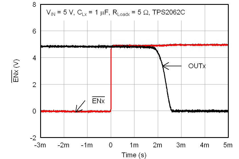
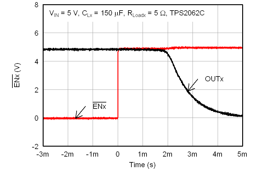
| toff | Turnoff time (2) | VIN = 5 V, CL = 1 µF, RL = 100 Ω, ENx ↑ or EN ↓ (see Figure 25, Figure 26, and Figure 23) 1 A, 1.5 A, 2 A Rated |
1.95 | 2.60 | 3.25 | ms | |
| tr | Rise time, output (2) | CL = 1 µF, RL = 100 Ω (see Figure 24) 1 A, 1.5 A, 2 A Rated |
0.58 | 0.82 | 1.15 | ms | |
| tf | Fall time, output (2) | CL = 1 µF, RL = 100 Ω (see Figure 24) 1 A, 1.5 A, 2 A Rated |
0.33 | 0.47 | 0.66 | ms | |
| CURRENT LIMIT | |||||||
| IOS | Current-limit (see Figure 28) | TPS2052C (0.5 A) | 0.7 | 1 | 1.3 | A | |
| TPS2062C, 62C-2, 66C, and 66C-2 (1 A) | 1.12 | 1.61 | 2.10 | ||||
| TPS2060C, 64C, and 64C-2 (1.5 A) | 1.72 | 2.29 | 2.86 | ||||
| TPS2002C and 03C (2 A) | 2.35 | 3.15 | 3.95 | ||||
| tIOS | Short-circuit response time | VIN = 5 V (see Figure 27), One-half full load → R(SHORT) = 50 mΩ, Measure from application to when current falls below 120% of final value |
2 | µs | |||
| SUPPLY CURRENT | |||||||
| ISD | Supply current, switch disabled | Standard conditions, I(OUTx) = 0 mA | 0.01 | 10 | µA | ||
| IS1E | Supply current, single switch enabled | Standard conditions, I(OUTx) = 0 mA | 90 | ||||
| IS2E | Supply current, both switches enabled | Standard conditions, I(OUTx) = 0 mA | 150 | ||||
| ILKG | Leakage current | VOUT = 0 V, VIN = 5.5 V, disabled, measured IVIN |
TPS20xxC-2 | 0.05 | |||
| Reverse leakage current | VOUT = 5.5 V, VIN = 0 V, measured I(OUTx) | 0.20 | |||||
| UNDERVOLTAGE LOCKOUT | |||||||
| UVLO | Low-level input voltage, IN | VIN rising | 3.4 | 4.0 | V | ||
| Hysteresis, IN | 0.14 | V | |||||
| FLTx | |||||||
| Output low voltage, FLTx | I(FLTx) = 1 mA | 0.2 | V | ||||
| Off-state leakage | V(FLTx) = 5.5 V | 1 | µA | ||||
| FLTx deglitch (2) | FLTx overcurrent assertion and deassertion | 7 | 10 | 13 | ms | ||
| OUTPUT DISCHARGE | |||||||
| Output pulldown resistance(2) | VIN = 5 V, VOUT = 5 V, disabled | TPS20xxC | 300 | 470 | 800 | Ω | |
| VIN = 4 V, VOUT = 5 V, disabled | TPS20xxC | 350 | 560 | 1200 | |||
| THERMAL SHUTDOWN | |||||||
| Junction thermal shutdown threshold | In current limit | 135 | °C | ||||
| Not in current limit | 155 | ||||||
| Hysteresis | 20 | °C | |||||
7.7 Typical Characteristics
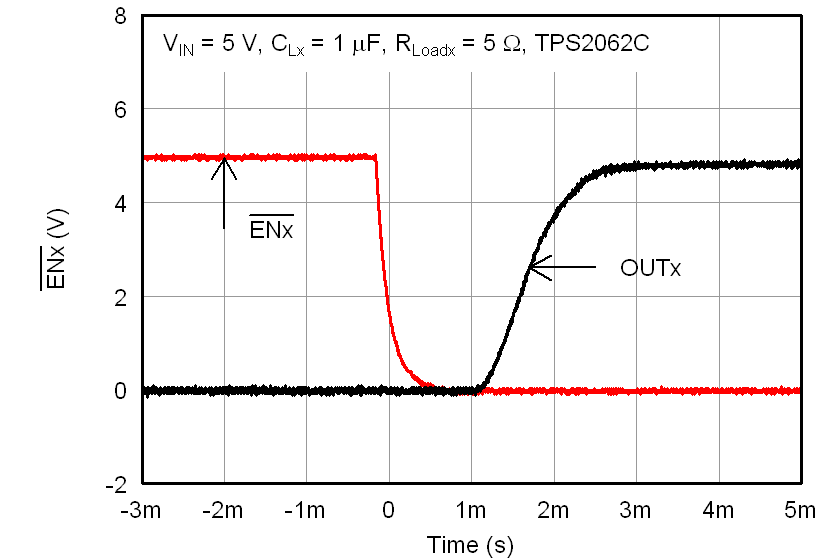
Rise Time With 1-μF Load
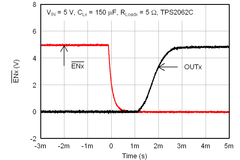
Rise Time With 150-μF Load
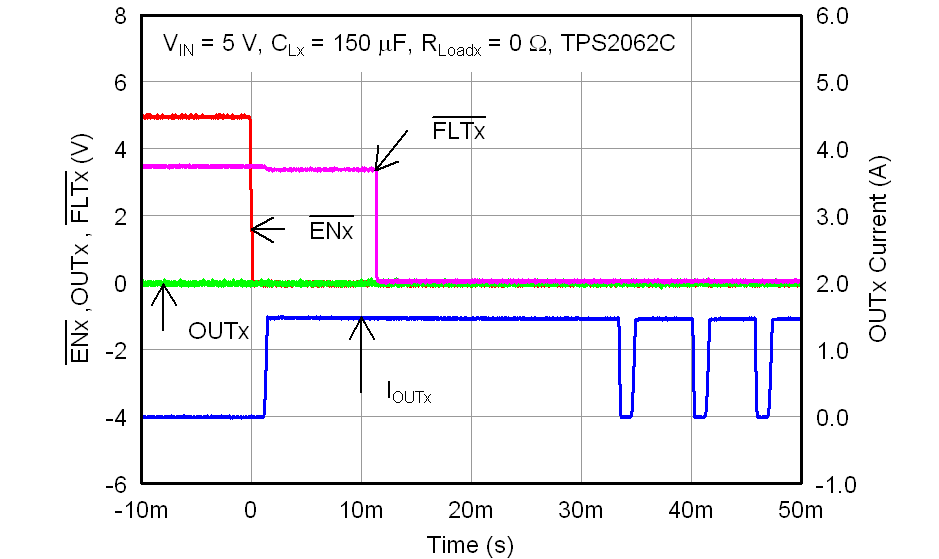
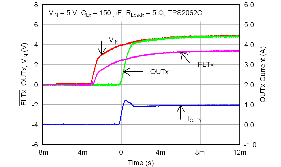
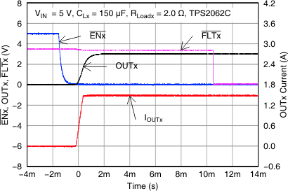
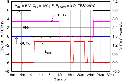
into Output Short
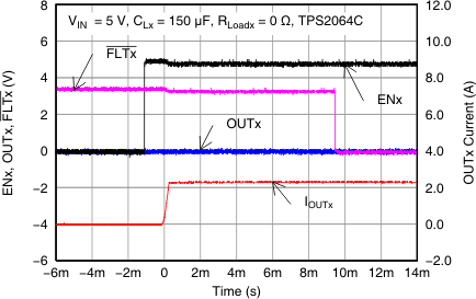
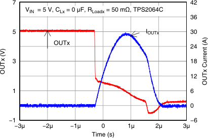
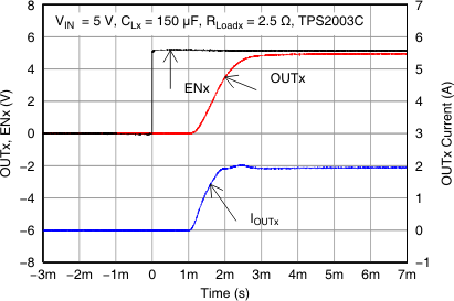
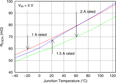
vs Temperature
Fall Time With 1-μF Load
Fall Time With 150-μF Load
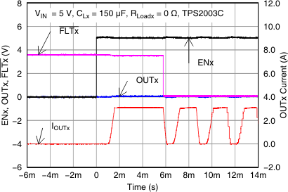
With Different Load Capacitance
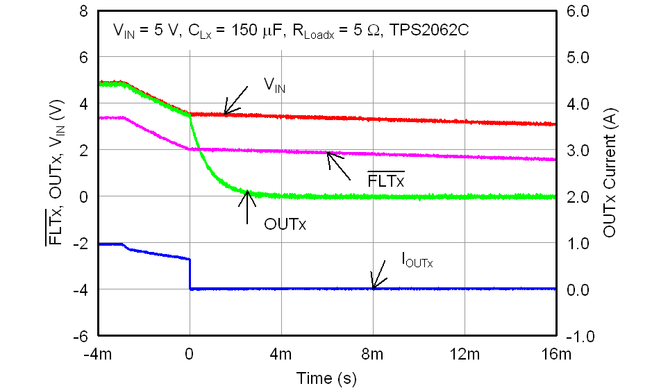
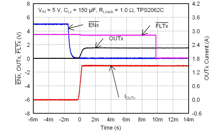
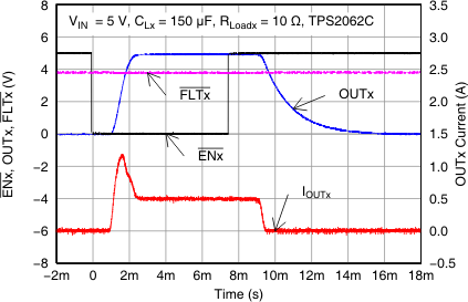
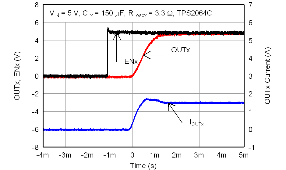
into 10-Ω Load
vs Temperature