SLVSAU6H June 2011 – April 2016 TPS2000C , TPS2001C , TPS2041C , TPS2051C , TPS2061C , TPS2065C , TPS2065C-2 , TPS2068C , TPS2069C , TPS2069C-2
PRODUCTION DATA.
- 1 Features
- 2 Applications
- 3 Description
- 4 Revision History
- 5 Device Comparison Table
- 6 Pin Configuration and Functions
-
7 Specifications
- 7.1 Absolute Maximum Ratings
- 7.2 ESD Ratings
- 7.3 Recommended Operating Conditions
- 7.4 Thermal Information: SOT-23
- 7.5 Thermal Information: MSOP-PowerPAD
- 7.6 Electrical Characteristics: TJ = TA = 25°C
- 7.7 Electrical Characteristics: -40°C ≤ TJ ≤ 125°C
- 7.8 Timing Requirements: TJ = TA = 25°C
- 7.9 Typical Characteristics
- 8 Detailed Description
- 9 Application and Implementation
- 10Power Supply Recommendations
- 11Layout
- 12Device and Documentation Support
- 13Mechanical, Packaging, and Orderable Information
8 Detailed Description
8.1 Overview
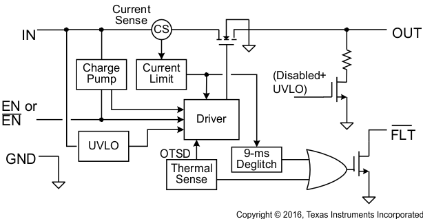
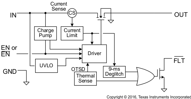
The TPS20xxC and TPS20xxC-2 are current-limited, power-distribution switches providing a range from 0.5 A and 2 A of continuous load current in 5-V circuits. These parts use N-channel MOSFETs for low resistance, maintaining voltage regulation to the load. They are designed for applications where short circuits or heavy capacitive loads are encountered. Device features include enable, reverse blocking when disabled, output discharge pulldown, overcurrent protection, overtemperature protection, and deglitched fault reporting.
8.2 Functional Block Diagram
 Figure 20. TPS20xxC Block Diagram
 Figure 21. TPS20xxC-2 Block Diagram
8.3 Feature Description
8.3.1 Undervoltage Lockout
The undervoltage lockout (UVLO) circuit disables the power switch until the input voltage reaches the UVLO turnon threshold. Built-in hysteresis prevents unwanted ON/OFF cycling due to input voltage drop from large current surges. FLT is high impedance when the TPS20xxC and TPS20xxC-2 are in UVLO.
8.3.2 Enable
The logic enable input (EN, or EN), controls the power switch, bias for the charge pump, driver, and other circuits. The supply current is reduced to less than 1 µA when the TPS20xxC and TPS20xxC-2 are disabled. Disabling the TPS20xxC and TPS20xxC-2 immediately clears an active FLT indication. The enable input is compatible with both TTL and CMOS logic levels.
The turnon and turnoff times (tON, tOFF) are composed of a delay and a rise or fall time (tR, tF). The delay times are internally controlled. The rise time is controlled by both the TPS20xxC and TPS20xxC-2 and the external loading (especially capacitance). TPS20xxC fall time is controlled by the loading (R and C), and the output discharge (RPD). TPS20xxC-2 does not have the output discharge (RPD), fall time is controlled by the loading (R and C). An output load consisting of only a resistor experiences a fall time set by the TPS20xxC and TPS20xxC-2. An output load with parallel R and C elements experiences a fall time determined by the (R × C) time constant if it is longer than the tF TPS20xxC and TPS20xxC-2.
The enable must not be left open, and may be tied to VIN or GND depending on the device.
8.3.3 Internal Charge Pump
The device incorporates an internal charge pump and gate drive circuitry necessary to drive the N-channel MOSFET. The charge pump supplies power to the gate driver circuit and provides the necessary voltage to pull the gate of the MOSFET above the source. The driver incorporates circuitry that controls the rise and fall times of the output voltage to limit large current and voltage surges on the input supply, and provides built-in soft-start functionality. The MOSFET power switch blocks current from OUT to IN when turned off by the UVLO or disabled.
8.3.4 Current Limit
The TPS20xxC and TPS20xxC-2 responds to overloads by limiting output current to the static IOS levels shown in Electrical Characteristics: TJ = TA = 25°C. When an overload condition is present, the device maintains a constant output current, with the output voltage determined by (IOS × RLOAD). Two possible overload conditions can occur. The first overload condition occurs when either:
- input voltage is first applied, enable is true, and a short circuit is present (load which draws IOUT > IOS)
- input voltage is present and the TPS20xxC and TPS20xxC-2 are enabled into a short circuit.
The output voltage is held near zero potential with respect to ground and the TPS20xxC and TPS20xxC-2 ramps the output current to IOS. The TPS20xxC and TPS20xxC-2 limits the current to IOS until the overload condition is removed or the device begins to thermal cycle. This is demonstrated in Figure 26 where the device was enabled into a short, and subsequently cycles current OFF and ON as the thermal protection engages.
The second condition is when an overload occurs while the device is enabled and fully turned on. The device responds to the overload condition within tIOS (Figure 5 and Figure 6) when the specified overload (see Electrical Characteristics: –40°C ≤ TJ ≤ 125°C) is applied. The response speed and shape varies with the overload level, input circuit, and rate of application. The current limit response will vary between simply settling to IOS, or turnoff and controlled return to IOS. Similar to the previous case, the TPS20xxC and TPS20xxC-2 limits the current to IOS until the overload condition is removed or the device begins to thermal cycle. This is demonstrated by Figure 27, Figure 28, and Figure 29.
The TPS20xxC and TPS20xxC-2 thermal cycles if an overload condition is present long enough to activate thermal limiting in any of the above cases. This is due to the relatively large power dissipation [(VIN – VOUT) × IOS] driving the junction temperature up. The device turns off when the junction temperature exceeds 135°C (minimum) while in current limit. The device remains off until the junction temperature cools 20°C and then restarts.
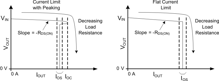
There are two kinds of current limit profiles typically available in TI switch products that are similar to the TPS20xxC and TPS20xxC-2. Many older designs have an output I vs V characteristic similar to the plot labeled Current Limit with Peaking in Figure 22. This type of limiting can be characterized by two parameters, the current limit corner (IOC), and the short circuit current (IOS). IOC is often specified as a maximum value. The TPS20xxC and TPS20xxC-2 family of parts does not present noticeable peaking in the current limit, corresponding to the characteristic labeled Flat Current Limit in Figure 22. This is why the IOC parameter is not present in Electrical Characteristics: –40°C ≤ TJ ≤ 125°C.
 Figure 22. Current Limit Profiles
8.3.5 FLT
The FLT open-drain output is asserted (active low) during an overload or overtemperature condition. A 9-ms deglitch on both the rising and falling edges avoids false reporting at start-up and during transients. A current limit condition shorter than the deglitch period clears the internal timer upon termination. The deglitch timer does not integrate multiple short overloads and declare a fault. This is also true for exiting from a faulted state. An input voltage with excessive ripple and large output capacitance may interfere with operation of FLT around IOS as the ripple drives the TPS20xxC and TPS20xxC-2 in and out of current limit.
If the TPS20xxC and TPS20xxC-2 are in current limit and the overtemperature circuit goes active, FLT goes true immediately (see Figure 27); however, the exiting this condition is deglitched (see Figure 29). FLT is tripped just as the knee of the constant-current limiting is entered. Disabling the TPS20xxC and TPS20xxC-2 clears an active FLT as soon as the switch turns off (see Figure 26). FLT is high impedance when the TPS20xxC and TPS20xxC-2 are disabled or in undervoltage lockout (UVLO).
8.3.6 Output Discharge
A 470-Ω (typical) output discharge dissipates stored charge and leakage current on OUT when the TPS20xxC is in UVLO or disabled. The pulldown circuit loses bias gradually as VIN decreases, causing a rise in the discharge resistance as VIN falls towards 0 V. The TPS20xxC-2 does not have this function. The output is be controlled by an external loadings when the device is in ULVO or disabled.
8.4 Device Functional Modes
There are no other functional modes.