SLVSAX6H October 2011 – December 2015 TPS2002C , TPS2003C , TPS2052C , TPS2060C , TPS2062C , TPS2062C-2 , TPS2064C , TPS2064C-2 , TPS2066C , TPS2066C-2
PRODUCTION DATA.
- 1 Features
- 2 Applications
- 3 Description
- 4 Revision History
- 5 Device Comparison Table
- 6 Pin Configuration and Functions
- 7 Specifications
- 8 Parameter Measurement Information
- 9 Detailed Description
- 10Application and Implementation
- 11Power Supply Recommendations
- 12Layout
- 13Device and Documentation Support
- 14Mechanical, Packaging, and Orderable Information
1 Features
- Dual Power Switch Family
- Rated Currents of 0.5 A, 1 A, 1.5 A, 2 A
- Accurate ±20% Current Limit Tolerance
- Fast Overcurrent Response – 2 µs (Typical)
- 70-mΩ (Typical) High-Side N-Channel MOSFET
- Operating Range: 4.5 V to 5.5 V
- Deglitched Fault Reporting (FLTx)
- Selected Parts With (TPS20xxC) and Without (TPS20xxC-2) Output Discharge
- Reverse Current Blocking
- Built-in Softstart
- Pin for Pin With Existing TI Switch Portfolio
- Ambient Temperature Range: –40°C to 85°C
2 Applications
- USB Ports or Hubs, Laptops, Desktops
- High-Definition Digital TVs
- Set Top Boxes
- Short Circuit Protection
3 Description
The TPS20xxC and TPS20xxC-2 dual power-distribution switch family is intended for applications such as USB where heavy capacitive loads and short-circuits may be encountered. This family offers multiple devices with fixed current-limit thresholds for applications between 0.5 A and 2 A.
The TPS20xxC and TPS20xxC-2 dual family limits the output current to a safe level by operating in a constant-current mode when the output load exceeds the current-limit threshold. This provides a predictable fault current under all conditions. The fast overcurrent response time eases the burden on the main 5 V supply to provide regulated power when the output is shorted. The power-switch rise and fall times are controlled to minimize current surges during turnon and turnoff.
Device Information(1)
| PART NUMBER | PACKAGE | BODY SIZE (NOM) |
|---|---|---|
| TPS2052C TPS2062C TPS2066C TPS2066C-2 TPS2060C TPS2064C TPS2064C-2 |
MSOP (8) | 3.00 mm × 3.00 mm |
| TPS2062C TPS2066C |
SOIC (8) | 3.90 mm × 4.90 mm |
| TPS2062C-2 | SON (8) | 3.00 mm × 3.00 mm |
| TPS2002C TPS2003C |
VSON (10) | 3.00 mm × 3.00 mm |
- For all available packages, see the orderable addendum at the end of the data sheet.
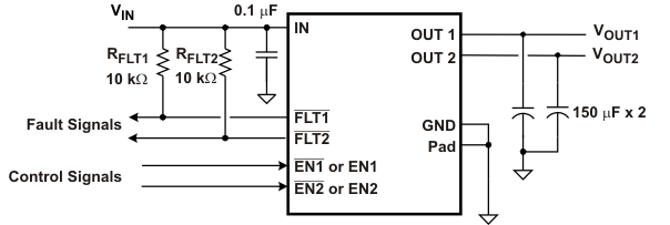
Typical Application
