JAJSG28F august 2018 – august 2020 TPS2120 , TPS2121
PRODUCTION DATA
- 1
- 1 特長
- 2 アプリケーション
- 3 概要
- 4 Revision History
- 5 Device Comparison Table
- 6 Pin Configuration and Functions
- 7 Specifications
- 8 Parameter Measurement Information
-
9 Detailed Description
- 9.1 Overview
- 9.2 Functional Block Diagram
- 9.3
Feature Description
- 9.3.1 Input Settling Time and Output Soft Start Control (SS)
- 9.3.2 Active Current Limiting (ILM)
- 9.3.3 Short-Circuit Protection
- 9.3.4 Thermal Protection (TSD)
- 9.3.5 Overvoltage Protection (OVx)
- 9.3.6 Fast Reverse Current Blocking (RCB)
- 9.3.7 Output Voltage Dip and Fast Switchover Control (TPS2121 only)
- 9.3.8 Input Voltage Comparator (VCOMP)
- 9.4 TPS2120 Device Functional Modes
- 9.5 TPS2121 Device Functional Modes
- 10Application and Implementation
- 11Power Supply Recommendations
- 12Layout
- 13Device and Documentation Support
- 14Mechanical, Packaging, and Orderable Information
パッケージ・オプション
デバイスごとのパッケージ図は、PDF版データシートをご参照ください。
メカニカル・データ(パッケージ|ピン)
- YFP|20
サーマルパッド・メカニカル・データ
発注情報
10.7 Hotplugging with TPS212x
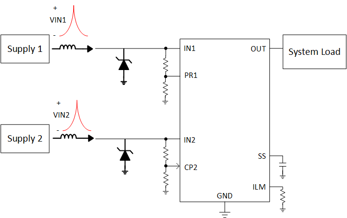
Some applications require power muxing between hotplugged inputs, such as USB applications or systems with secondary supplies coming from a long cable. During a hot plug event, the inherent inductance in the cable and input traces can cause a voltage spike on the input pin (V = LCABLE * dI / dT). This can cause a voltage spike on the input of the TPS212x that could potentially exceed the absolute maximum rating.
 Figure 10-20 TPS212x Hotplug Configuration
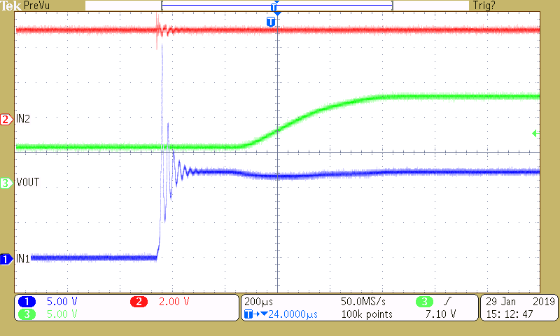
Figure 10-21 shows a hotplug event where a 12-V supply is connected to the TPS212x through a 15ft cable. Without an external TVS, the input voltage spikes to over 30 V. To protect against this voltage transient, a clamping device such as a TVS (Transient Voltage Suppression) diode can be used. As shown in Figure 10-22 , by using the TVS1800, the same voltage spike was clamped to 19.3 V.
 Figure 10-21 TPS2121 Hotplug Event without TVS
 Figure 10-22 TPS2121 Hotplug Event with TVS1800