SLVSCX7A February 2015 – March 2015 TPS22958
PRODUCTION DATA.
- 1 Features
- 2 Applications
- 3 Description
- 4 Revision History
- 5 Device Comparison Table
- 6 Pin Configuration and Functions
-
7 Specifications
- 7.1 Absolute Maximum Ratings
- 7.2 ESD Ratings
- 7.3 Recommended Operating Conditions
- 7.4 Thermal Information
- 7.5 Electrical Characteristics (VBIAS = 5 V)
- 7.6 Electrical Characteristics (VBIAS = 3.3 V)
- 7.7 Electrical Characteristics (VBIAS = 2.5 V)
- 7.8 Switching Characteristics
- 7.9 Typical DC Characteristics
- 7.10 Typical AC Characteristics
- 8 Parameter Measurement Information
- 9 Detailed Description
- 10Application and Implementation
- 11Power Supply Recommendations
- 12Layout
- 13Device and Documentation Support
- 14Mechanical, Packaging, and Orderable Information
パッケージ・オプション
メカニカル・データ(パッケージ|ピン)
サーマルパッド・メカニカル・データ
- DGN|8
発注情報
10 Application and Implementation
10.1 Application Information
10.1.1 Input Capacitor (Optional)
To limit the voltage drop on the input supply caused by transient inrush currents when the switch turns on into a discharged load capacitor, a capacitor can be placed between VIN and GND. A 1 µF ceramic capacitor, CIN, placed close to the pins, is usually sufficient. Higher values of CIN can be used to further reduce the voltage drop during high-current application. When switching heavy loads, TI recommends to have an input capacitor about 10× higher than the output capacitor to avoid excessive voltage drop.
10.1.2 Output Capacitor (Optional)
Due to the integrated body diode in the NMOS switch, TI recommends a CIN greater than CL. A CL greater than CIN can cause the voltage on VOUT to exceed VIN when the system supply is removed. This could result in current flow through the body diode from VOUT to VIN. TI recommends a CIN to CL ratio of 10 to 1 for minimizing VIN dip caused by inrush currents during startup.
10.1.3 Power Supply Sequencing Without a GPIO Input
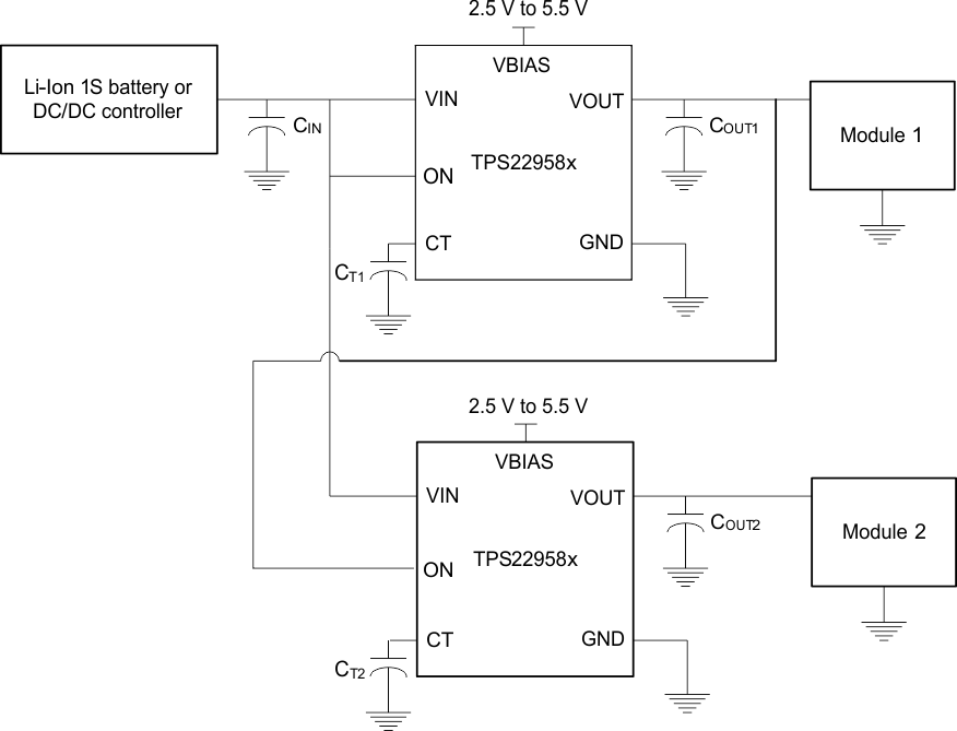 Figure 36. Power Supply Sequencing Without a GPIO Input
In many end equipments, there is a need to power up various modules in a pre-determined manner. The TPS22958x can solve the problem of power sequencing without adding any complexity to the overall system. Figure 36 shows the configuration required for powering up two modules in a fixed sequence. The output of the first load switch is tied to the enable of the second load switch, so when Module 1 is powered the second load switch is enabled and Module 2 is powered.
10.2 Typical Application
This application demonstrates how the TPS22958 can be used to power a downstream load with a large capacitance. The example in Figure 37 is powering a 22 µF capacitive output load.
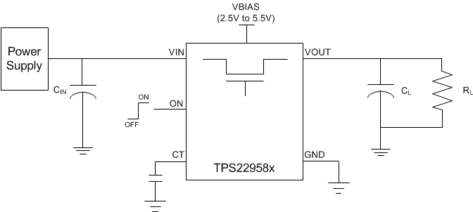 Figure 37. Typical Application Schematic
10.2.1 Design Requirements
For this design example, use the following as the input parameters.
Table 3. Design Parameters
| DESIGN PARAMETER | EXAMPLE VALUE |
|---|---|
| VIN | 3.3 V |
| VBIAS | 5.0 V |
| Load current | 4 A |
| Output capacitance (CL) | 22 µF |
| Allowable inrush current on VOUT | 0.33 A |
10.2.2 Detailed Design Procedure
To begin the design process, the designer needs to know the following:
- VIN voltage
- VBIAS voltage
- Load current
- Allowable inrush current on VOUT due to CL capacitor
10.2.2.1 VIN to VOUT Voltage Drop
The VIN to VOUT voltage drop in the device is determined by the RON of the device and the load current. The RON of the device depends upon the VIN and VBIAS conditions of the device. Refer to the RON specification of the device in the Electrical Characteristics table. After the RON of the device is determined based upon the VIN and VBIAS conditions, use Equation 2 to calculate the VIN to VOUT voltage drop:

where
- ΔV = voltage drop from VIN to VOUT
- ILOAD = load current
- RON = On-resistance of the device for a specific VIN and VBIAS combination
An appropriate ILOAD must be chosen such that the IMAX specification of the device is not violated.
10.2.2.2 Inrush Current
To determine how much inrush current will be caused by the CL capacitor, use Equation 3.

where
- IINRUSH = amount of inrush caused by CL
- CL = capacitance on VOUT
- dt = time it takes for change in VOUT during the ramp up of VOUT when the device is enabled
- dVOUT = change in VOUT during the ramp up of VOUT when the device is enabled
The device offers adjustable rise time for VOUT and allows the user to control the inrush current during turn-on through the CT pin. The appropriate rise time can be calculated using the design requirements and the inrush current equation (Equation 3).
To ensure an inrush current of less than 330 mA, choose a CT based on Table 1 or Equation 1 value that will yield a rise time of more than 220 µs. See the oscilloscope captures in the Application Curves for an example of how the CT capacitor can be used to reduce inrush current. See Table 1 for correlation between rise times and CT values.
An appropriate CL value should be placed on VOUT such that the IMAX and IPLS specifications of the device are not violated.
10.2.2.3 Thermal Considerations
The maximum IC junction temperature should be restricted to 125°C under normal operating conditions. To calculate the maximum allowable dissipation, PD(max) for a given output current and ambient temperature, use Equation 7.

where
- PD(max) = maximum allowable power dissipation
- TJ(max) = maximum allowable junction temperature (125°C for the TPS22958)
- TA = ambient temperature of the device
- RθJA = junction to air thermal impedance. See Thermal Information. This parameter is highly dependent upon board layout.
For the DGK package, VBIAS = 5 V, and VIN = 3.3 V, the maximum ambient temperature with a 4 A load can be determined by using the following calculation:
Therefore, with the conditions mentioned above, a maximum ambient temperature of 65.6°C is recommended.
For the DGN package, VBIAS = 5 V, and VIN = 3.3 V, the maximum ambient temperature with a 4 A load can be determined by using the following calculation:
Therefore, with the conditions mentioned above, a maximum ambient temperature of 103.6°C is recommended.
10.2.3 Application Curves
The three scope captures show the usage of a CT capacitor in conjunction with the device. A higher CT value results in a slower rise and a lower inrush current.
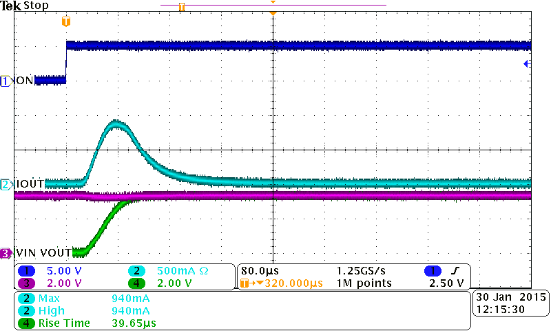
| VBIAS = 5 V | VIN = 3.3 V | TA = 25°C |
| CT = Open | CL = 22µF |
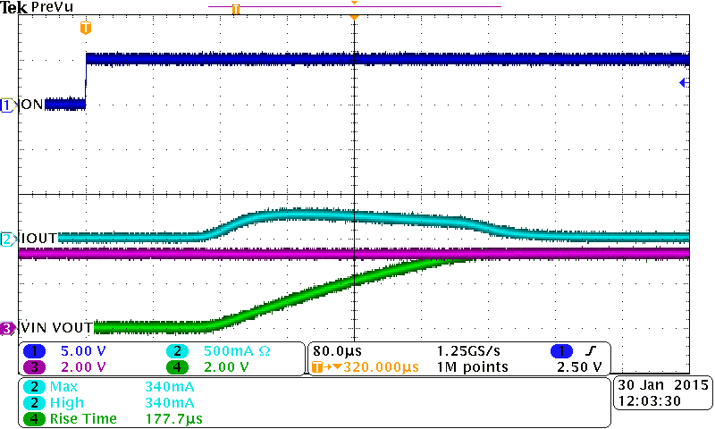
| VBIAS = 5 V | VIN = 3.3 V | |||
| CT = 470 pF | CL = 22µF | TA = 25°C |
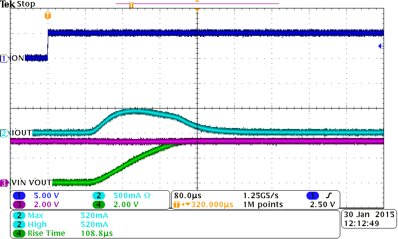
| VBIAS = 5 V | VIN = 3.3 V | TA = 25°C |
| CT = 220 pF | CL = 22µF |