JAJSGL9C October 2013 – December 2018 TPS24750 , TPS24751
UNLESS OTHERWISE NOTED, this document contains PRODUCTION DATA.
- 1 特長
- 2 アプリケーション
- 3 概要
- 4 改訂履歴
- 5 Device Comparison Table
- 6 Pin Configuration and Functions
- 7 Specifications
- 8 Parameter Measurement Information
-
9 Detailed Descriptions
- 9.1 Overview
- 9.2 Functional Block Diagram
- 9.3 Feature Description
- 9.4 Device Functional Modes
-
10Application and Implementation
- 10.1 Application Information
- 10.2
Typical Application
- 10.2.1 Design Requirements
- 10.2.2
Detailed Design Procedure
- 10.2.2.1
Power-Limited Start-Up
- 10.2.2.1.1 STEP 1. Choose RSENSE, RSET, and RIMON
- 10.2.2.1.2 STEP 2. Choose Power-Limit Value, PLIM, and RPROG
- 10.2.2.1.3 STEP 3. Choose Output Voltage Rising Time, tON, and Timing Capacitor CT
- 10.2.2.1.4 STEP 4. Calculate the Retry-Mode Duty Ratio
- 10.2.2.1.5 STEP 5. Select R1, R2, and R3 for UV and OV
- 10.2.2.1.6 STEP 6. Choose R4, R5, and C1
- 10.2.2.2 Alternative Design Example: Gate Capacitor (dv/dt) Control in Inrush Mode
- 10.2.2.3 Additional Design Considerations
- 10.2.2.1
Power-Limited Start-Up
- 10.2.3 Application Curves
- 10.3 System Examples
- 11Power Supply Recommendations
- 12Layout
- 13デバイスおよびドキュメントのサポート
- 14メカニカル、パッケージ、および注文情報
パッケージ・オプション
メカニカル・データ(パッケージ|ピン)
- RUV|36
サーマルパッド・メカニカル・データ
- RUV|36
発注情報
10.2.2.1.1 STEP 1. Choose RSENSE, RSET, and RIMON
The recommended range of the current-limit threshold voltage, V(VCC – SENSE), extends from 10 mV to 42 mV. Values near the low threshold of 10 mV may be affected by system noise. Values near the upper threshold of 42 mV may be too close to the minimum fast-trip threshold voltage of 52 mV. Values near the middle of this range help minimize both concerns.
To achieve high efficiency, the power dissipation in RSENSE must be kept to a minimum. A RSENSE of 2 mΩ develops a voltage of 22 mV at the specified peak current limit of 11 A, while dissipating only 200 mW at the rated 10-A current. This represents a 0.17% power loss.
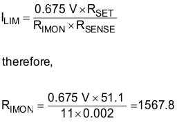
For best performance, a current of approximately 0.5 mA (see the Recommended Operatings Conditions table) must flow into the SET pin and out of the IMON pin when the TPS2475x is in current limit. The voltage across RSET nominally equals the voltage across RSENSE, or 22 mV. Dividing 22 mV by 0.5 mA gives a recommended value of RSET of 44 Ω. A 51.1-Ω, 1% resistor was chosen. Using Equation 3, the value of RIMON must equal 1568 Ω, or as near as practically possible. A 1.58-kΩ, 1% resistor was chosen. See Equation 5.
