JAJS440B November 2009 – December 2016 TPS2556 , TPS2557
PRODUCTION DATA.
- 1 特長
- 2 アプリケーション
- 3 概要
- 4 改訂履歴
- 5 Device Comparison Table
- 6 Pin Configuration and Functions
- 7 Specifications
- 8 Parameter Measurement Information
- 9 Detailed Description
-
10Application and Implementation
- 10.1 Application Information
- 10.2
Typical Applications
- 10.2.1 Current-Limiting Power-Distribution Switch
- 11Power Supply Recommendations
- 12Layout
- 13デバイスおよびドキュメントのサポート
- 14メカニカル、パッケージ、および注文情報
パッケージ・オプション
メカニカル・データ(パッケージ|ピン)
- DRB|8
サーマルパッド・メカニカル・データ
- DRB|8
発注情報
10 Application and Implementation
NOTE
Information in the following applications sections is not part of the TI component specification, and TI does not warrant its accuracy or completeness. TI’s customers are responsible for determining suitability of components for their purposes. Customers should validate and test their design implementation to confirm system functionality.
10.1 Application Information
The TPS2556 and TPS2557 are precision power-distribution switches for applications where heavy capacitive loads and short circuits are expected to be encountered. The following design procedures can be used to choose the input and output capacitors as well as to calculate the current limit programming resistor value for a typical design. Additional application examples are provided including an auto-retry circuit and a two-level current limit circuit.
10.2 Typical Applications
10.2.1 Current-Limiting Power-Distribution Switch
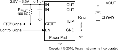 Figure 18. Typical Current-Limiting Application
10.2.1.1 Design Requirements
For this example, use the parameters listed in Table 1 as the input parameters.
Table 1. Design Parameters
| PARAMETER | VALUE |
|---|---|
| Input voltage | 5 V |
| Output voltage | 5 V |
| Above a minimum current limit | 3000 mA |
| Below a maximum current limit | 5000 mA |
10.2.1.2 Detailed Design Procedure
10.2.1.2.1 Input and Output Capacitance
Input and output capacitance improves the performance of the device; the actual capacitance must be optimized for the particular application. TI recommends a 0.1-µF or greater ceramic bypass capacitor between IN and GND as close to the device as possible for local noise decoupling for all applications. This precaution reduces ringing on the input due to power-supply transients. Additional input capacitance may be needed on the input to reduce voltage overshoot from exceeding the absolute-maximum voltage of the device during heavy transient conditions. This is especially important during bench testing when long, inductive cables are used to connect the evaluation board to the bench power supply.
Output capacitance is not required, but TI recommends placing a high-value electrolytic capacitor on the output pin when large transient currents are expected on the output.
10.2.1.2.2 Programming the Current-Limit Threshold
The overcurrent threshold is user programmable through an external resistor. The TPS255x uses an internal regulation loop to provide a regulated voltage on the ILIM pin. The current-limit threshold is proportional to the current sourced out of ILIM. The recommended 1% resistor for RILIM is 20 kΩ ≤ RILIM ≤ 187 kΩ to ensure stability of the internal regulation loop. Many applications require that the minimum current limit is above a certain current level or that the maximum current limit is below a certain current level, so it is important to consider the tolerance of the overcurrent threshold when selecting a value for RILIM. Equation 1 approximates the resulting overcurrent threshold for a given external resistor value (RILIM). See Electrical Characteristics for specific current limit settings. The traces routing the RILIM resistor to the TPS255x must be as short as possible to reduce parasitic effects on the current-limit accuracy.
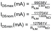
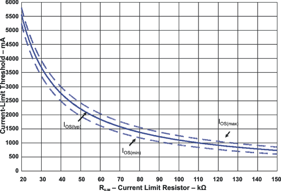 Figure 19. Current-Limit Threshold vs RILIM
10.2.1.2.2.1 Designing Above a Minimum Current Limit
Some applications require that current limiting cannot occur below a certain threshold. For this example, assume that 3 A must be delivered to the load so that the minimum desired current-limit threshold is 3000 mA. Use the IOS equations and Figure 19 to select RILIM.
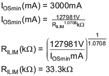
Select the closest 1% resistor less than the calculated value: RILIM = 33.2 kΩ. This sets the minimum current-limit threshold at 3000 mA . Use the IOS equations, Figure 19, and the previously calculated value for RILIM to calculate the maximum resulting current-limit threshold.
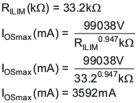
The resulting maximum current-limit threshold is 3592 mA with a 33.2-kΩ resistor.
10.2.1.2.2.2 Designing Below a Maximum Current Limit
Some applications require that current limiting must occur below a certain threshold. For this example, assume that the desired upper current-limit threshold must be below 5000 mA to protect an upstream power supply. Use the IOS equations and Figure 19 to select RILIM.
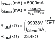
Select the closest 1% resistor greater than the calculated value: RILIM = 23.7 kΩ. This sets the maximum current-limit threshold at 5000 mA . Use the IOS equations, Figure 19, and the previously calculated value for RILIM to calculate the minimum resulting current-limit threshold.
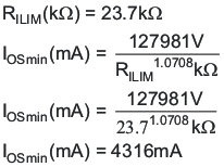
The resulting minimum current-limit threshold is 4316 mA with a 23.7-kΩ resistor.
10.2.1.2.2.3 Accounting for Resistor Tolerance
The analysis of resistor selection focused only on the TPS255x performance and assumed an exact resistor value. However, resistors sold in quantity are not exact and are bounded by an upper and lower tolerance centered around a nominal resistance. The additional RILIM resistance tolerance directly affects the current-limit threshold accuracy at a system level. Table 2 shows a process that accounts for worst-case resistor tolerance assuming 1% resistor values. Using the selection process outlined, determine the upper and lower resistance bounds of the selected resistor. Then calculate the upper and lower resistor bounds to determine the threshold limits. It is important to use tighter tolerance resistors (0.5% or 0.1%) when precision current limiting is desired.
Table 2. Common RILIM Resistor Selections
| DESIRED NOMINAL CURRENT LIMIT (mA) | IDEAL RESISTOR (kΩ) | CLOSEST 1% RESISTOR (kΩ) | RESISTOR BOUNDS (kΩ) | IOS ACTUAL LIMITS (mA) | |||
|---|---|---|---|---|---|---|---|
| 1% LOW | 1% HIGH | MIN | NOM | MAX | |||
| 750 | 146.9 | 147 | 145.5 | 148.5 | 605 | 749 | 886 |
| 1000 | 110.2 | 110 | 108.9 | 111.1 | 825 | 1002 | 1166 |
| 1250 | 88.2 | 88.7 | 87.8 | 89.6 | 1039 | 1244 | 1430 |
| 1500 | 73.6 | 73.2 | 72.5 | 73.9 | 1276 | 1508 | 1715 |
| 1750 | 63.1 | 63.4 | 62.8 | 64 | 1489 | 1742 | 1965 |
| 2000 | 55.2 | 54.9 | 54.4 | 55.4 | 1737 | 2012 | 2252 |
| 2250 | 49.1 | 48.7 | 48.2 | 49.2 | 1975 | 2269 | 2523 |
| 2500 | 44.2 | 44.2 | 43.8 | 44.6 | 2191 | 2501 | 2765 |
| 2750 | 40.2 | 40.2 | 39.8 | 40.6 | 2425 | 2750 | 3025 |
| 3000 | 36.9 | 36.5 | 36.1 | 36.9 | 2689 | 3030 | 3315 |
| 3250 | 34 | 34 | 33.7 | 34.3 | 2901 | 3253 | 3545 |
| 3500 | 31.6 | 31.6 | 31.3 | 31.9 | 3138 | 3501 | 3800 |
| 3750 | 29.5 | 29.4 | 29.1 | 29.7 | 3390 | 3764 | 4068 |
| 4000 | 27.7 | 27.4 | 27.1 | 27.7 | 3656 | 4039 | 4349 |
| 4250 | 26 | 26.1 | 25.8 | 26.4 | 3851 | 4241 | 4554 |
| 4500 | 24.6 | 24.9 | 24.7 | 25.1 | 4050 | 4446 | 4761 |
| 4750 | 23.3 | 23.2 | 23 | 23.4 | 4369 | 4773 | 5091 |
| 5000 | 22.1 | 22.1 | 21.9 | 22.3 | 4602 | 5011 | 5331 |
| 5250 | 21.1 | 21 | 20.8 | 21.2 | 4861 | 5274 | 5595 |
| 5500 | 20.1 | 20 | 19.8 | 20.2 | 5121 | 5539 | 5859 |
10.2.1.2.3 Auto-Retry Functionality
Some applications require that an overcurrent condition disables the part momentarily during a fault condition and re-enables after a pre-set time. This auto-retry functionality can be implemented with an external resistor and capacitor. During a fault condition, FAULTpulls EN low. The part is disabled when EN is pulled below the turn-off theshold, and FAULT goes high impedance allowing CRETRY to begin charging. The part re-enables when the voltage on EN reaches the turn-on threshold. The auto-retry time is determined by the resistor and capacitor time constant. The part continues to cycle in this manner until the fault condition is removed. The time between retries is given in Equation 6.
where
- VEN is the EN pin typical threshold voltage
- VIN is the input voltage
- VOL is the FAULT pin typical saturation voltage
- TFAULT is the internal FAULT typical deglitch time
The retry duty cycle is calculated with Equation 7, and the average current is D × IOS.
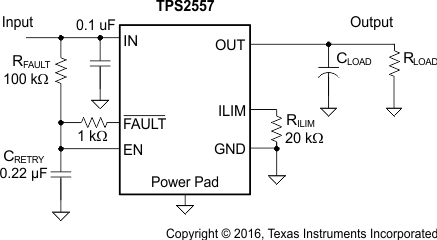 Figure 20. Auto-Retry Functionality
Some applications require auto-retry functionality and the ability to enable and disable with an external logic signal. The figure below shows how an external logic signal can drive EN through RFAULT and maintain auto-retry functionality. The resistor and capacitor time constant determines the auto-retry time-out period.
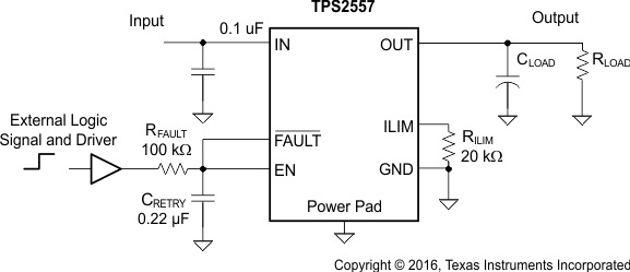 Figure 21. Auto-Retry Functionality With External EN Signal
10.2.1.2.4 Two-Level Current-Limit Circuit
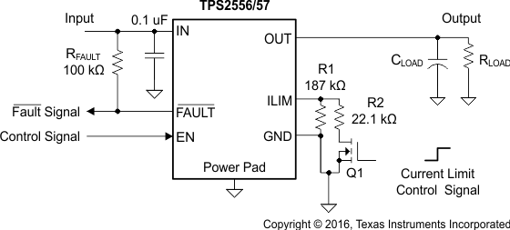 Figure 22. Two-Level Current-Limit Circuit
Some applications require different current-limit thresholds depending on external system conditions. Figure 22 shows an implementation for an externally-controlled, two-level current-limit circuit. The current-limit threshold is set by the total resistance from ILIM to GND (see Programming the Current-Limit Threshold). A logic-level input enables and disables MOSFET Q1 and changes the current-limit threshold by modifying the total resistance from ILIM to GND. Additional MOSFET and resistor combinations can be used in parallel to Q1 and R2 to increase the number of additional current-limit levels.
NOTE
ILIM must never be driven directly with an external signal.
10.2.1.3 Application Curve
In Figure 23, the load current setpoint is 5.05 A, as programmed by the 22.1-kΩ resistor. Load current is stepped mildly from approximately 4.9 A to 5.2 A. The internal FAULT timer runs and after 9 ms, FAULT goes low and current continues to be regulated at approximately 5 A. Due to the high power dissipation within the device, thermal cycling occurs.
In Figure 24, the load current setpoint is 597 mA, as programmed by the 187-kΩ resistor. Load current is stepped mildly from approximately 560 mA to 620 mA. The internal FAULT timer runs and after 9 ms, FAULT goes low and current continues to be regulated at approximately 580 mA.
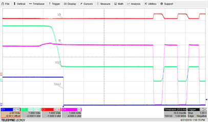 Figure 23. 5-A Current Limit With Thermal Cycling
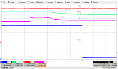 Figure 24. 600-mA Current Limit Without Thermal Cycling