SLVSDG8B April 2016 – June 2017 TPS25740 , TPS25740A
PRODUCTION DATA.
- 1 Features
- 2 Applications
- 3 Description
- 4 Revision History
- 5 Device Comparison Table
- 6 Pin Configuration and Functions
- 7 Specifications
-
8 Detailed Description
- 8.1 Overview
- 8.2 Functional Block Diagram
- 8.3
Feature Description
- 8.3.1 USB Type-C CC Logic (CC1, CC2)
- 8.3.2 USB PD BMC Transmission (CC1, CC2, VTX)
- 8.3.3 USB PD BMC Reception (CC1, CC2)
- 8.3.4 Discharging (DSCG, VPWR)
- 8.3.5 Configuring Voltage Capabilities (HIPWR, EN9V, EN12V)
- 8.3.6 Configuring Power Capabilities (PSEL, PCTRL, HIPWR)
- 8.3.7 Gate Driver (GDNG, GDNS)
- 8.3.8 Fault Monitoring and Protection
- 8.3.9 Voltage Control (CTL1, CTL2)
- 8.3.10 Sink Attachment Indicator (UFP, DVDD)
- 8.3.11 Power Supplies (VAUX, VDD, VPWR, DVDD)
- 8.3.12 Grounds (AGND, GND)
- 8.3.13 Output Power Supply (DVDD)
- 8.4 Device Functional Modes
-
9 Application and Implementation
- 9.1
Application Information
- 9.1.1 System-Level ESD Protection
- 9.1.2 Use of GD Internal Clamp
- 9.1.3 Resistor Divider on GD for Programmable Start Up
- 9.1.4 Selection of the CTL1 and CTL2 Resistors (R(FBL1) and R(FBL2))
- 9.1.5 Voltage Transition Requirements
- 9.1.6 VBUS Slew Control using GDNG C(SLEW)
- 9.1.7 Tuning OCP Using RF and CF
- 9.2 Typical Application , A/C Power Source (Wall Adapter)
- 9.3 System Examples
- 9.1
Application Information
- 10Power Supply Recommendations
- 11Layout
- 12Device and Documentation Support
- 13Mechanical, Packaging, and Orderable Information
パッケージ・オプション
メカニカル・データ(パッケージ|ピン)
- RGE|24
サーマルパッド・メカニカル・データ
- RGE|24
発注情報
9 Application and Implementation
NOTE
Information in the following applications sections is not part of the TI component specification, and TI does not warrant its accuracy or completeness. TI’s customers are responsible for determining suitability of components for their purposes. Customers should validate and test their design implementation to confirm system functionality.
9.1 Application Information
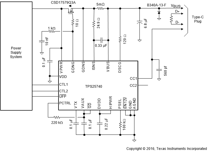
The TPS25740 or TPS25740A implements a fully compliant USB Power Delivery 2.0 provider and Type-C source (also known as downward facing port (DFP)). The device basic schematic diagram is shown in Figure 36. Subsequent sections describe detailed design procedures for several applications with differing requirements. The TPS25740/TPS25740A Design Calculator Tool (refer to the Documentation Support) is available for download and use in calculating the equations in the following sections.
9.1.1 System-Level ESD Protection
System-level ESD (per EN61000-4-2) may occur as the result of a cable being plugged in, or a user touching the USB connector or cable. Figure 37 shows an example ESD protection for the VBUS path that helps protect the VBUS pin, ISNS and DSCG pins of the device from system-level ESD. The device has ESD protection built into the CC1 and CC2 pins so that no external protection is necessary. Refer to the Layout Guidelines section for external component placement and routing recommendations.
The Schottky diode is to protect against VBUS being drawn below ground by an inductive load, the cable inductance may be as high as 900 nH.
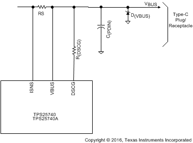 Figure 37. VBUS ESD Protection
9.1.2 Use of GD Internal Clamp
As described in the Configuring Power Capabilities (PSEL, PCTRL, HIPWR) section, the GD pin has an internal clamp. Figure 38 shows an example of how it may be used. VOUT is the voltage from a power supply that is to be provided onto the VBUS wire of the USB Type-C cable through an NFET resistor. If VOUT drops, the NFET should be automatically disabled by the device. This can be accomplished by tying the GD pin to VOUT via a resistor.
The internal resistance of the GD pin is specified to exceed R(GD), and the input threshold is V(GD_TH). The GD pin would therefore draw no more than V(GD_TH) max / R(GD) min < 603 nA. As an example, assume the minimum value of VOUT for which GD should be high is 4.5 V, then the resistor between GD and VOUT may not exceed (4.5 – V(GD_TH) max) / 603e-9 = 4.5 MΩ. To make it robust against board leakage a smaller resistor such as 1 MΩ can be chosen, but the smaller the resistance the more leakage current into the GD pin. In this example, when VOUT is 25 V, the current into the GD pin is (25-V(GDC)) / 1e6 < 1.85 µA.
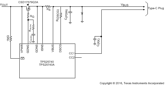 Figure 38. Use of GD Internal Clamp
9.1.3 Resistor Divider on GD for Programmable Start Up
Figure 39 shows an alternative usage of the GD pin can help protect against shorts on the VBUS pin in the receptacle. A resistor divider is used to minimize the time it takes the GD pin to be pulled low. Consider the situation where the VBUS pin is shorted at startup. At some point, the device closes the NFET switch to supply 5 V to VBUS. At that point, the short pulls down on the voltage seen at the VPWR pin. With the resistor values shown in Figure 39, once the voltage at the VPWR pin reaches 3.95 V the voltage at the GD pin is specified to be below V(GD_TH) min. Without the 700-kΩ resistor, the voltage at the VPWR pin would have to reach V(GD_TH) min which takes longer. This comes at the expense of increased leakage current.
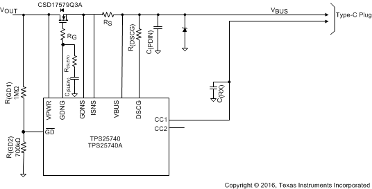 Figure 39. Programmable GD Turn On
The GD resistor values can be calculated using the following process. First, calculate the smallest R(GD1) that should be used to prevent the internal clamp current from exceeding I(GD) of 80 µA. For a 20 V advertised voltage, the OVP trip point could be as high as 24 V. Using V(GDC) min = 6.5 V and VOUT = V(FOVP20) max = 24 V, provides Equation 3:

The actual clamping current is less than 80 µA as some current flows into R(GD2). Next, R(GD2) can be calculated as shown in Equation 4:

where
- V(VPWR) = V(VPWR_TH) falling (max) and V(GD_TH) = V(GD_TH) falling (min).
9.1.4 Selection of the CTL1 and CTL2 Resistors (R(FBL1) and R(FBL2))
R(FBL1) and R(FBL2) provide a means to change the power supply output voltage when switched in by the CTL1 and CTL2 open drain outputs, respectively. When 12 V is requested by the UFP then CTL2 will go low and place R(FBL2) in parallel with R(FBL). When 20 V is requested by the UFP then CTL2 remains low and CTL1 goes low placing R(FBL1) in parallel with R(FBL2) and R(FBL).
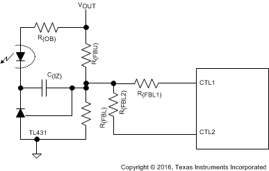 Figure 40. Circuit to Change VOUT Upon Sink/UFP Request
R(FBL2) is calculated using Equation 5. In this example, VOUT12 is 12 V and VOUT20 is 20 V. VOUT is the default output voltage (5 V) for the regulator and is set by R(FBU), R(FBL) and error amplifier VREF.

R(FBL1) is calculated using Equation 6 after a standard 1% value for R(FBL2) is chosen.

R(FBL1) and R(FBL2) should be large enough so that the CTL1 and CTL2 sinking current is minimized (< 1 mA). The sinking current for CTL1 and CTL2 is VREF / R(FBL1) and VREF/R(FBL2) respectively.
9.1.5 Voltage Transition Requirements
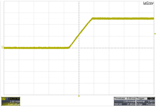
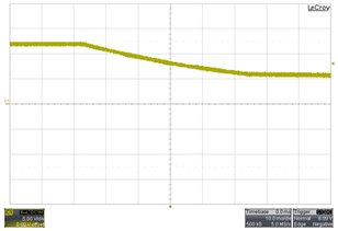
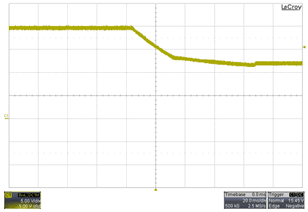
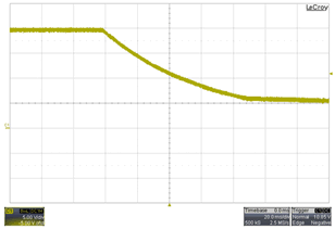
During VBUS voltage transitions, the slew rate (vSrcSlewPos) must be kept below 30 mV/µs in all portions of the waveform, settle (tSrcSettle) in less than 275 ms, and be ready (tSrcReady) in less than 285 ms. For most power supplies, these requirements are met naturally without any special circuitry but in some cases, the voltage transition ramp rate must be slowed in order to meet the slew rate requirement.
The requirements for linear voltage transitions are shown in Table 7. In all cases, the minimum slew time is below 1 ms.
Table 7. Minimum Slew-Rate Requirements
| Voltage Transition | 5 V ↔ 12 V | 5 V ↔ 20 V | 12 V ↔ 20 V | 5 V ↔ 9 V | 5 V ↔ 15 V | 9 V ↔ 15 V |
| Minimum Slew Time | 233 µs | 500 µs | 267 µs | 133 µs | 333 µs | 200 µs |
When transition slew control is required, the interaction of the slew mechanism and dc/dc converter loop response must be considered. A simple R-C filter between the device CTL pins and converter feedback node may lead to instability under some conditions. Figure 41 shows a method which manages the slew control without adding capacitance to the converter feedback node.
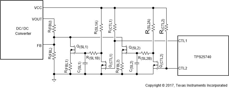 Figure 41. Slew-Rate Control Example No. 1
When VOUT = 5 V, both CTL1 and CTL2 are in a high impedance state. When a 5 V to 12 V transition is requested, CTL2 goes low and turns off Q(CTL2). Q(SL2) gate starts to rise towards VCC at a rate determined by R(SL2A) + R(SL2B) and C(SL2). Q(SL2) gate continues to rise, until Q(SL2) is fully enhanced placing R(FBL2) in parallel with R(FBL). In similar fashion when C(TL1) goes low, Q(CTL1) turns off allowing R(FBL1) to slew in parallel with R(FBL2) and R(FBL).
The slewing resistors and capacitor can be chosen using the following equations. VT is the VGS threshold voltage of Q(SL1) and Q(SL2). VREF is the feedback regulator reference voltage. Choose the slewing resistance in the 100 kΩ range to reduce the loading on the bias voltage source (VCC) and then calculate C(SL). The falling transitions is shorter than the rising transitions in this topology.
Falling transitions:
- 20 V to 12 V

- 12 V to 5 V

Rising transitions:
- 5 V to 12 V

- 12 V to 20 V

Some converter regulators can tolerate a balance of capacitance on the feedback node without affecting loop stability. The LM5175 has been tested using Figure 42 to combine VOUT slewing with a minimal amount of extra circuitry.
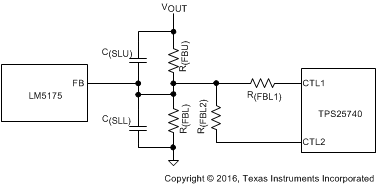 Figure 42. Slew-Rate Control Example No. 2
When a higher voltage is requested from TPS25740, CTL1 or CTL2 goes low changing the sensed voltage at the FB pin. The LM5175 compensates by increasing C(SLU). As VOUT increases, C(SLU) is charged at a rate proportional to R(FBU). Three time constants yields a voltage change of approximately 95% and can be used to calculate the desired slew time. C(SLU) can be calculated using Equation 11 and Equation 12.


In order to minimize loop stability effects, a capacitor in parallel with R(FBL) is required. The ratio of C(SLU)/C(SLL) should be chosen to match the ratio of R(FBL)/R(FBU). Choose C(SLL) according to Equation 13.

All slew rate control methods should be verified on the bench to ensure that the slew rate requirements are being met when the external VBUS capacitance is between 1 μF and 100 μF.
9.1.6 VBUS Slew Control using GDNG C(SLEW)
Care should be taken to control the slew rate of Q1 using C(SLEW); particularly in applications where COUT >> C(SLEW). The slew rate observed on VBUS when charging a purely capacitive load is the same as the slew rate of V(GDNG) and is dominated by the ratio I(GDNON) / C(SLEW). R(SLEW) helps block C(SLEW) from the GDNG pin enabling a faster transient response to OCP.
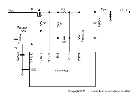 Figure 43. Slew-Rate control Using GDNG
There may be fault conditions where the voltage on VBUS triggers an OVP condition and then remains at a high voltage even after the TPS25740 configures the voltage source to output 5 V via CTL1 and CTL2. When this OVP occurs, the TPS25740 opens Q1 within tFOVP + tFOVPDG. The TPS25740 then issues a hard reset, discharge the power-path via the R(DSCG), and waits for 795 ms before enabling Q1 again. Due to the fault condition the voltage again triggers an OVP event when the voltage on VBUS exceeds V(FOVP). This retry process would continue as long as the fault condition persists, periodically pulsing up to V(FOVP) + VSrcSlewPos x (tFOVP + tFOVPDG) onto the VBUS of the Type-C receptacle. It is recommended to use a slew rate less than the maximum of VSrcSlewPos (30 mV / µs) allowed by USB (refer to Documentation Support), the slew rate should instead be set in order to meet the requirement to have the voltage reach the target voltage within tSrcSettle (275 ms). This also limits the out-rush current from the COUT capacitor into the C(PDIN) capacitor and help protect Q1 and RS.
9.1.7 Tuning OCP Using RF and CF
In applications where there are load transients or moderate ripple on VOUT, the OCP performance of TPS25740 or TPS25740A may be impacted. Adding the RF/CF filter network as shown in Figure 44 helps mitigate the impact of the ripple and load transients on OCP performance.
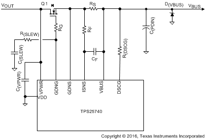 Figure 44. ISNS Filtering Example
RF/CF can be tailored to the amount of ripple on VOUT as shown in Table 8.
Table 8. Ripple on VOUT
| Frequency x Ripple (kHz x V) | Suggested Filter Time Constant (µs) |
|---|---|
| < 5 (Ex: 50 mV ripple at 100 kHz) | None |
| 5 to 15 | 2.2 µs ( RF = 10 Ω, CF = 220 nF) |
| 15 to 35 | 4.7 µs ( RF = 10 Ω, CF = 470 nF) |
| 35 to 105 | 10 µs ( RF = 10 Ω, CF = 1 µF) |
9.2 Typical Application , A/C Power Source (Wall Adapter)
In this design example, PSEL pin is configured so that P(SEL) = 65 W (see Table 9). Voltages offered are 5 V, 12 V, and 20 V at a maximum of 3 A. The overcurrent protection (OCP) trip point is set just above 3 A and VDD on the TPS25740 is grounded. The following example is based on PMP11451 and PMP11455, see www.ti.com/tool/PMP11451. In this design, the TPS25740 and some associated discretes are located on the paddle card (PMP11455) which plugs into the power supply card (PMP11451). This allows different paddle cards with different power and voltage advertisements to be used with a common power supply design.
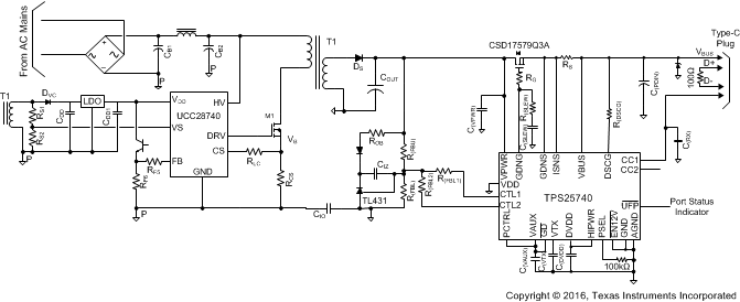 Figure 45. Captive Cable Adapter Provider Conceptual Schematic
9.2.1 Design Requirements
Table 9. Design Parameters
| Design Parameter | Value |
|---|---|
| Configured Power Limit, P(SEL) | 65 W |
| Advertised Voltages | 5 V, 12 V, 20 V |
| Advertised Current Limit | 3 A |
| Over Current Protection Set point | 4.2 A |
9.2.2 Detailed Design Procedure
9.2.2.1 Power Pin Bypass Capacitors
- C(VPWR): 0.1 μF, 50 V, ±10%, X7R ceramic at pin 20 (VPWR)
- C(VDD): 0.1 μF, 50 V, X7R ceramic at pin 17 (VDD). If VDD is not used in the application, then tie VDD to GND.
- C(DVDD): 0.22 μF, 10 V, ±10%, X5R ceramic at pin 13 (DVDD)
- C(VAUX): 0.1 μF, 50 V, ±10%, X7R ceramic at pin 16 (VAUX)
- C(VTX): 0.1 μF, 50 V, ±10%, X7R ceramic at pin 1 (VTX)
9.2.2.2 Non-Configurable Components
- R(SEL): When the application requires advertisement using R(SEL) , use a 100 kΩ, ±1% resistor.
- R(PCTRL): If PCTRL will be pulled low with an external device then it can be connected to VAUX using a 220 kΩ, ±1% resistor. If PCTRL is always high, then it can be directly connected to VAUX.
- R(SLEW): Use a 1 kΩ, ±1% resistor
- RG: Use a 10 Ω, ±1% resistor
9.2.2.3 Configurable Components
- C(RX): Choose C(RX) between 200 pF and 600 pF. A 560 pF, 50 V, ±5% COG/NPO ceramic is recommended for both CC1 and CC2 pins.
- Q1: For a 3 A application, an N-Channel MOSFET with RDS(on) in the 10 mΩ range is sufficient. BV(DSS) should be rated for 30 V for applications delivering 20 V, and 25 V for 12 V applications. For this application, the TI CSD17579Q3A (SLPS527) NexFET™ is suitable.
- RS: TPS25740 or TPS25740A OCP set point thresholds are targeted towards a 5 mΩ, ±1% sense resistor. Power dissipation for RS at 3 A load is approximately 45 mW.
- R(DSCG): The minimum value of R(DSCG) is chosen based on the application VBUS (max) and I(DSCGT). For VBUS (max) = 12 V and I(DSCGT) = 350 mA, R(DSCG(min)) = 34.3 Ω. The size of the external resistor can then be chosen based on the capacitive load that needs to be discharged and the maximum allowed discharge time of 265 ms. Typically, a 120 Ω, 0.5 W resistor provides suitable performance.
- RF/CF: Not used
- C(PDIN): The requirement for C(PDIN) is 10 µF maximum. A 6.8 µF, 25 V, ±10% X5R or X7R ceramic capacitor is suitable for most applications.
- D(VBUS): D(VBUS) provides reverse transient protection during large transient conditions when inductive loads are present. A Schottky diode with a V(RRM) rating of 30 V in a SMA package such as the B340A-13-F provideds suitable reverse voltage clamping performance.
- C(SLEW): To achieve a slew rate from zero to 5 V of less than 30 mV / µs using the typical GDNG current of 20 µA then C(SLEW) > 20 µA / 30 mV / µs = 0.67 nF be used. Choosing C(SLEW) = 10 nF yields a ramp rate of 2 mV / µs.
- R(FBL1)/R(FBL2): In this design example, R(FBU) = 20 kΩ and R(FBL) = 20 kΩ. The feedback error amplifier is TL431AI which is rated for up to 36 V operation and VREF = 2.495 V. Using the equations for R(FBL2) above yields a calculated value of 7.1 kΩ and a selected value of 7.15 kΩ. In similar fashion for R(FBL1), the equations yield a calculated value of 6.35 kΩ and a selected value of 6.34 kΩ.
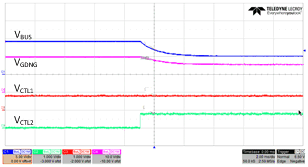
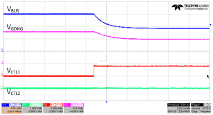
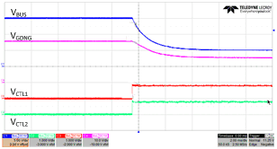
9.2.3 Application Curves
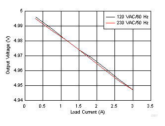
| DFP End - VBUS = 5 V | ||
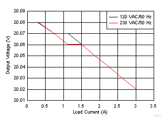
| DFP End - VBUS = 20 V | ||
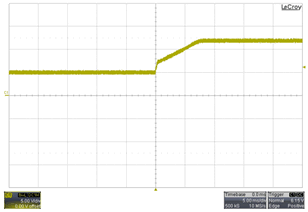
| No Load |
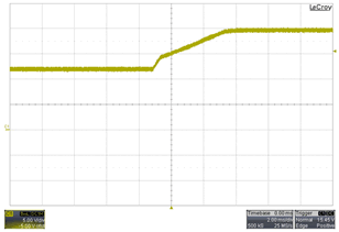
| No Load |
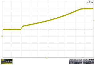
| No Load |
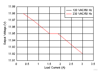
| DFP End - VBUS = 12 V | ||
| No Load |
| No Load |
| No Load |
| No Load |
9.2.4 Typical Application, D/C Power Source
In this design example the PSEL pin is configured such that P(SEL) = 65 W (see Table 10). Voltages offered are 5 V, 9 V, and 15 V at a maximum of 3 A. The overcurrent protection (OCP) trip point is set just above 3 A and VDD on the TPS25740A is grounded. The following example is based on TPS25740AEVM-741 (refer to Documentation Support).
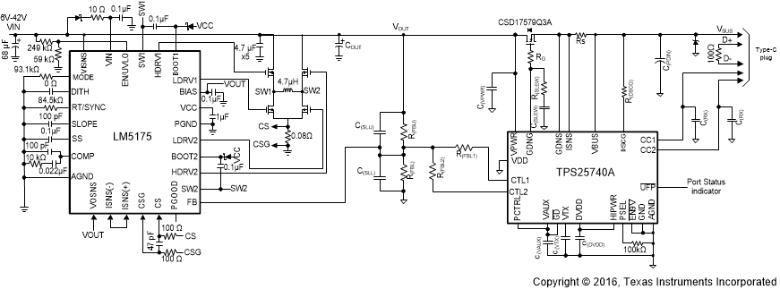 Figure 56. DC Power Source
9.2.4.1 Design Requirements
Table 10. Design Parameters
| Design Parameter | Value |
|---|---|
| Configured Power Limit, P(SEL) | 65 W |
| Advertised Voltages | 5 V, 9 V, 15 V |
| Advertised Current Limit | 3 A |
| Over Current Protection Set point | 4.2 A |
9.2.4.2 Detailed Design Procedure
9.2.4.2.1 Power Pin Bypass Capacitors
- C(VPWR): 0.1 μF, 50 V, ±10%, X7R ceramic at pin 20 (VPWR)
- C(VDD): 0.1 μF, 50 V, X7R ceramic at pin 17 (VDD). If VDD is not used in the application, then tie VDD to GND.
- C(DVDD): 0.22 μF, 10 V, ±10%, X5R ceramic at pin 13 (DVDD)
- C(VAUX): 0.1 μF, 50 V, ±10%, X7R ceramic at pin 16 (VAUX)
- C(VTX): 0.1 μF, 50 V, ±10%, X7R ceramic at pin 1 (VTX)
9.2.4.2.2 Non-Configurable Components
- R(SEL): When the application requires advertisement using R(SEL) , use a 100 kΩ, ±1% resistor.
- R(PCTRL): If PCTRL will be pulled low with an external device then it can be connected to VAUX using a 220 kΩ, ±1% resistor. If PCTRL will always be high then it can be directly connected to VAUX.
- R(SLEW): Use a 1 kΩ, ±1% resistor
- RG: Use a 10 Ω, ±1% resistor
9.2.4.2.3 Configurable Components
- C(RX): Choose C(RX) between 200 pF and 600 pF. A 560 pF, 50 V, ±5% COG/NPO ceramic is recommended for both CC1 and CC2 pins.
- Q1: For a 3 A application, an N-Channel MOSFET with RDS(on) in the 10 mΩ range is sufficient. BV(DSS) should be rated for 30 V for applications delivering 20 V, and 25 V for 12 V applications. For this application, the TI CSD17579Q3A (SLPS527) NexFET™ is suitable.
- RS: TPS25740 or TPS25740A OCP set point thresholds are targeted towards a 5 mΩ, ±1% sense resistor. Power dissipation for RS at 3 A load is approximately 45 mW.
- R(DSCG): The minimum value of R(DSCG) is chosen based on the application VBUS (max) and I(DSCGT). For VBUS (max) = 12 V and I(DSCGT) = 350 mA, RDS(CG(min)) = 34.3 Ω. The size of the external resistor can then be chosen based on the capacitive load that needs to be discharged and the maximum allowed discharge time of 265 ms. Typically, a 120 Ω, 0.5 W resistor provides suitable performance.
- RF/CF: Not used
- C(PDIN): The requirement for C(PDIN) is 10 µF maximum. A 6.8 µF, 25 V, ±10% X5R or X7R ceramic capacitor is suitable for most applications.
- D(VBUS): D(VBUS) provides reverse transient protection during large transient conditions when inductive loads are present. A Schottky diode with a V(RRM) rating of 30 V in a SMA package such as the B340A-13-F provideds suitable reverse voltage clamping performance.
- C(SLEW): To achieve a slew rate from zero to 5 V of less than 30 mV / µs using the typical GDNG current of 20 µA then C(SLEW) (nF) > 20 µA / 30 mV / µs = 0.67 nF be used. Choosing C(SLEW) = 10 nF yields a ramp rate of 2 mV / µs.
- R(FBL1)/R(FBL2): In this design example, R(FBU) = 49.9 kΩ and R(FBL) = 9.53 kΩ. The feedback error amplifier VREF = 0.8 V. Using the equations for R(FBL2) (Equation 5 and Equation 6) provide a calculated value of 9.9 kΩ and a selected value of 9.76 kΩ. In similar fashion for R(FBL1), a calculated value of 6.74 kΩ and a selected value of 6.65 kΩ is provided.
- C(SLU)/C(SLL): The value of C(SLU) is calculated based on the desired 95% slew rate using Equation 12 and Equation 13. Choose a 22 nF capacitor for C(SLU). Choose a 100 nF capacitor for C(SLL).
9.2.4.3 Application Curves
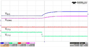
| No Load |
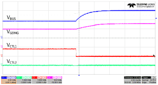
| No Load |
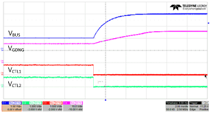
| No Load |
| No Load |
| No Load |
| No Load |
9.3 System Examples
9.3.1 D/C Power Source (Power Hub)
In this system design example, the P(SEL) is configured such that P(SEL) = 93 W and 5 V, 12 V or 20 V are offered at a maximum of 5 A. The over-current protection (OCP) trip point is set just above 5 A.
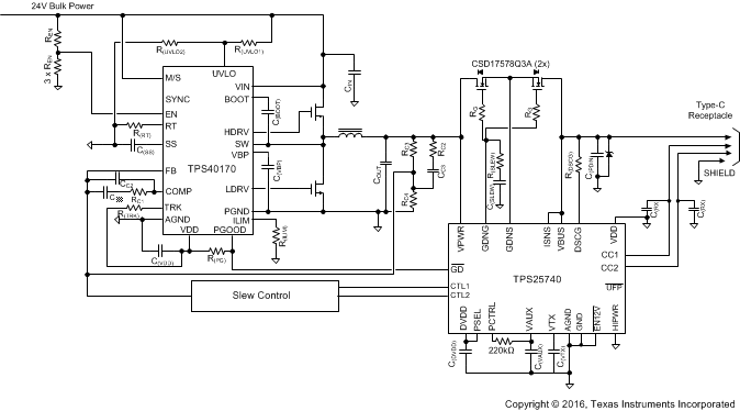 Figure 63. Power Hub Concept (Provider only)
This power hub circuit takes a 24 V input and produces a regulated output voltage. The over-current protection feature in the TPS25740 is not used; the ISNS and VBUS pins are connected directly. Instead R(ILIM) is chosen to set the current limit of the TPS40170 synchronous PWM buck controller. If the current limit trips, the GD pin of the TPS25740 is pulled low by the PGOOD pin of the TPS40170, which causes the power-path switch to be opened. Other fault conditions may also pull PGOOD low, but the slew rate of the voltage transition should be controlled as in one of the examples given above (Figure 41, Figure 42, or Figure 43).
VDD on the TPS25740 is grounded, if there is a suitable power supply available in the system the TPS25740 operates more efficiently if it is connected to VDD since V(VPWR) > V(VDD). See Figure 66 for an example.
9.3.2 A/C Power Source (Wall Adapter)
In this system design example, the PSEL pin is configured such that P(SEL) = 36 W, and only 5 V and 12 V are offered at a maximum of 3 A. The overcurrent protection (OCP) trip point is set just above 3 A. VDD on the TPS25740 is grounded, if there is a suitable power supply available in the system the TPS25740 operates more efficiently if it is connected to VDD since V(VPWR) > V(VDD).
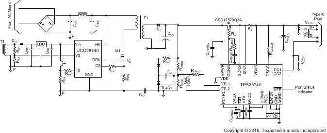 Figure 64. Adapter Provider Concept
9.3.3 Dual-Port Power Managed A/C Power Source (Wall Adaptor)
In this system design example, the PSEL pin is configured such that P(SEL) = 36 W, and only 5 V and 12 V are offered at a maximum of 3 A. The over-current protection (OCP) trip point is set just above 3 A.
The UFP pin from one TPS25740 is attached to the PCTRL pin on the other TPS25740. When one port is not active (no UFP attached through the receptacle) its UFP pin is left high-z so the PCTRL pin on the other port is pulled high. This allows the adaptor to provide up to the full 36 W on a single port if a single UFP is attached. If two UFP’s are attached (one to each port) then each port only offers current that would reach a maximum of 18 W. So each port is allocated half of the overall power when each port has a UFP attached.
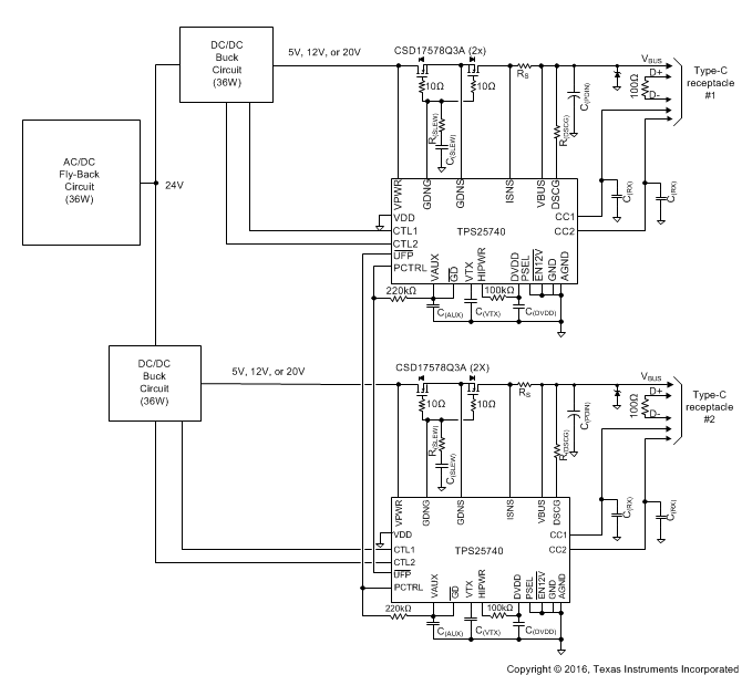 Figure 65. Dual-Port Adapter Provider Concept
9.3.4 D/C Power Source (Power Hub with 3.3 V Rail)
In Figure 66, an LDO that outputs at least I(SUPP) at 3.3 V or 5 V is added to the power hub concept, and the DVDD pin is used to enable the buck regulator since it is active high. For an active low buck regulator, the UFP pin could be used. This implementation is more power efficient than the one in Figure 63.
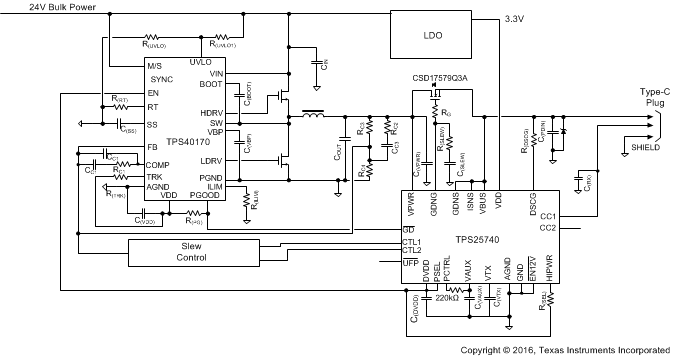 Figure 66. Power Hub Concept (Provider only)
