JAJSCH0D August 2016 – January 2018 TPS25741 , TPS25741A
UNLESS OTHERWISE NOTED, this document contains PRODUCTION DATA.
- 1 特長
- 2 アプリケーション
- 3 概要
- 4 改訂履歴
- 5 Device Comparison Table
- 6 Pin Configuration and Functions
- 7 Specifications
-
8 Detailed Description
- 8.1 Overview
- 8.2 Functional Block Diagram
- 8.3
Feature Description
- 8.3.1 USB Type-C CC Logic (CC1, CC2)
- 8.3.2 9.3.2 VCONN Supply (VCONN, CC1, CC2)
- 8.3.3 USB Power Delivery BMC Transmission (CC1, CC2, VTX)
- 8.3.4 USB Power Delivery BMC Reception (CC1, CC2)
- 8.3.5 Discharging (DSCG, VPWR)
- 8.3.6 Configuring Voltage Capabilities (HIPWR, EN9V, EN12V)
- 8.3.7 Configuring Power Capabilities (PSEL, PCTRL, HIPWR)
- 8.3.8 Gate Drivers
- 8.3.9 Fault Monitoring and Protection
- 8.3.10 Voltage Control (CTL1, CTL2)
- 8.3.11 Sink Attachment Indicator (UFP, DVDD)
- 8.3.12 Accessory Attachment Indicator (AUDIO, DEBUG)
- 8.3.13 Plug Polarity Indication (POL)
- 8.3.14 Power Supplies (VAUX, VDD, VPWR, DVDD)
- 8.3.15 Grounds (AGND, GND)
- 8.3.16 Output Power Supply (DVDD)
- 8.4 Device Functional Modes
- 9 Application and Implementation
- 10Power Supply Recommendations
- 11Layout
- 12デバイスおよびドキュメントのサポート
- 13メカニカル、パッケージ、および注文情報
パッケージ・オプション
メカニカル・データ(パッケージ|ピン)
- RSM|32
サーマルパッド・メカニカル・データ
- RSM|32
発注情報
9.1.4 Selection of the CTL1 and CTL2 Resistors (RFBL1 and RFBL2)
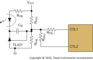
RFBL1 and RFBL2 provide a means to change the power supply output voltage when switched in by the CTL1 and CTL2 open drain outputs, respectively. When 12 V is requested by the UFP then CTL2 will go low and place RFBL2 in parallel with RFBL. When 20 V is requested by the UFP then CTL2 remains low and CTL1 goes low placing RFBL1 in parallel with RFBL2 and RFBL.
 Figure 45. Circuit to Change VOUT Upon Sink/UFP Request
RFBL2 is calculated using Equation 4. In this example, VOUT12 is 12 V and VOUT20 is 20 V. VOUT is the default output voltage (5 V) for the regulator and is set by RFBU, RFBL, and error amplifier VREF.

RFBL1 is calculated using the equation below after a standard 1% value for RFBL2 is chosen.

RFBL1 and RFBL2 should be large enough so that the CTL1/CTL2 sinking current is minimized (< 1 mA). The sinking current for CTL1 and CTL2 is VREF / RFBL1 and VREF/RFBL2 respectively.