JAJSCH0D August   2016  – January 2018 TPS25741 , TPS25741A

UNLESS OTHERWISE NOTED, this document contains PRODUCTION DATA.  

  1. 特長
  2. アプリケーション
  3. 概要
    1.     Device Images
      1.      DFPホスト・ポートへの実装の簡略図
  4. 改訂履歴
  5. Device Comparison Table
  6. Pin Configuration and Functions
    1.     Pin Functions
  7. Specifications
    1. 7.1 Absolute Maximum Ratings
    2. 7.2 ESD Ratings
    3. 7.3 Recommended Operating Conditions
    4. 7.4 Thermal Information
    5. 7.5 Electrical Characteristics
    6. 7.6 Timing Requirements
    7. 7.7 Switching Characteristics
    8. 7.8 Typical Characteristics
  8. Detailed Description
    1. 8.1 Overview
      1. 8.1.1 VBUS Capacitance
      2. 8.1.2 USB Data Communications
    2. 8.2 Functional Block Diagram
    3. 8.3 Feature Description
      1. 8.3.1  USB Type-C CC Logic (CC1, CC2)
      2. 8.3.2  9.3.2 VCONN Supply (VCONN, CC1, CC2)
      3. 8.3.3  USB Power Delivery BMC Transmission (CC1, CC2, VTX)
      4. 8.3.4  USB Power Delivery BMC Reception (CC1, CC2)
      5. 8.3.5  Discharging (DSCG, VPWR)
        1. 8.3.5.1 Discharging after a Fault (VPWR)
      6. 8.3.6  Configuring Voltage Capabilities (HIPWR, EN9V, EN12V)
      7. 8.3.7  Configuring Power Capabilities (PSEL, PCTRL, HIPWR)
      8. 8.3.8  Gate Drivers
        1. 8.3.8.1 GDNG, GDNS
        2. 8.3.8.2 G5V
        3. 8.3.8.3 GDPG
      9. 8.3.9  Fault Monitoring and Protection
        1. 8.3.9.1 Over/Under Voltage (VBUS)
        2. 8.3.9.2 Over-Current Protection (ISNS, VBUS)
        3. 8.3.9.3 System Fault Input (GD, VPWR)
      10. 8.3.10 Voltage Control (CTL1, CTL2)
      11. 8.3.11 Sink Attachment Indicator (UFP, DVDD)
      12. 8.3.12 Accessory Attachment Indicator (AUDIO, DEBUG)
      13. 8.3.13 Plug Polarity Indication (POL)
      14. 8.3.14 Power Supplies (VAUX, VDD, VPWR, DVDD)
      15. 8.3.15 Grounds (AGND, GND)
      16. 8.3.16 Output Power Supply (DVDD)
    4. 8.4 Device Functional Modes
      1. 8.4.1 Sleep Mode
      2. 8.4.2 Checking VBUS at Start Up
  9. Application and Implementation
    1. 9.1 Application Information
      1. 9.1.1 System-Level ESD Protection
      2. 9.1.2 Use of GD Internal Clamp
      3. 9.1.3 Resistor Divider on GD for Programmable Start Up
      4. 9.1.4 Selection of the CTL1 and CTL2 Resistors (RFBL1 and RFBL2)
      5. 9.1.5 Voltage Transition Requirements
      6. 9.1.6 VBUS Slew Control using GDNG CSLEW
      7. 9.1.7 Tuning OCP Using RF and CF
    2. 9.2 Typical Applications
      1. 9.2.1 A/C Multiplexing Power Source
        1. 9.2.1.1 Design Requirements
        2. 9.2.1.2 Detailed Design Procedure
          1. 9.2.1.2.1 Power Pin Bypass Capacitors
          2. 9.2.1.2.2 Non-Configurable Components
          3. 9.2.1.2.3 Configurable Components
        3. 9.2.1.3 Application Curves
      2. 9.2.2 D/C Power Source
        1. 9.2.2.1 Design Requirements
        2. 9.2.2.2 Detailed Design Procedure
          1. 9.2.2.2.1 Power Pin Bypass Capacitors
          2. 9.2.2.2.2 Non-Configurable Components
          3. 9.2.2.2.3 Configurable Components
        3. 9.2.2.3 Application Curves
    3. 9.3 System Examples
      1. 9.3.1 A/C Power Source (Wall Adapter)
      2. 9.3.2 Dual-Port Power Managed A/C Power Source (Wall Adapter)
  10. 10Power Supply Recommendations
    1. 10.1 VDD
    2. 10.2 VCONN
    3. 10.3 VPWR
  11. 11Layout
    1. 11.1 Layout Guidelines
      1. 11.1.1 Port Current Kelvin Sensing
      2. 11.1.2 Power Pin Bypass Capacitors
      3. 11.1.3 Supporting Components
    2. 11.2 Layout Example
  12. 12デバイスおよびドキュメントのサポート
    1. 12.1 ドキュメントのサポート
    2. 12.2 関連リンク
    3. 12.3 ドキュメントの更新通知を受け取る方法
    4. 12.4 コミュニティ・リソース
    5. 12.5 商標
    6. 12.6 静電気放電に関する注意事項
    7. 12.7 Glossary
  13. 13メカニカル、パッケージ、および注文情報

パッケージ・オプション

メカニカル・データ(パッケージ|ピン)
サーマルパッド・メカニカル・データ
発注情報

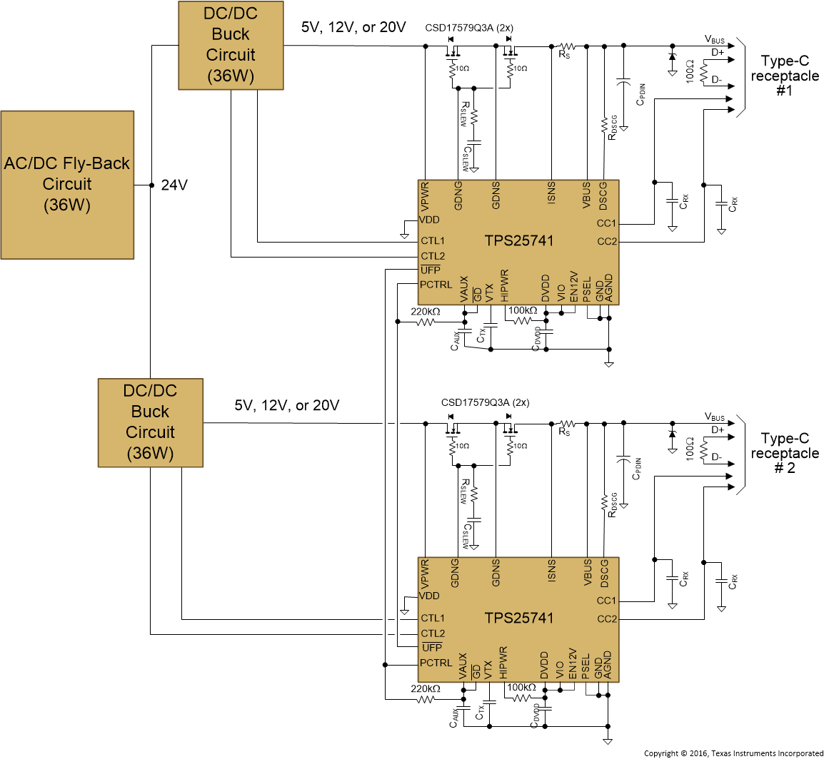
Dual-Port Power Managed A/C Power Source (Wall Adapter)

In this system design example, the PSEL is configured such that PSEL = 36 W, and only 5 V and 12 V are offered at a maximum of 3 A. The over-current protection (OCP) trip point is set just above 3 A.

The UFP pin from one TPS25741 is attached to the PCTRL pin on the other TPS25741. When one port is not active (no UFP attached through the receptacle) its UFP pin is left high-z so the PCTRL pin on the other port is pulled high. This allows the adaptor to provide up to the full 36 W on a single port if a single UFP is attached. If two UFP’s are attached (one to each port) then each port only offers current that would reach a maximum of 18 W. So each port is allocated half of the overall power when each port has a UFP attached.
TPS25741 TPS25741A Dual_prt_adapt_slvsdj5.gifFigure 72. Dual-Port Adapter Provider Concept