JAJS461A October 2009 – November 2016 TPS54290 , TPS54291 , TPS54292
PRODUCTION DATA.
- 1 特長
- 2 アプリケーション
- 3 概要
- 4 改訂履歴
- 5 Device Comparison Table
- 6 Pin Configuration and Functions
- 7 Specifications
-
8 Detailed Description
- 8.1 Overview
- 8.2 Functional Block Diagram
- 8.3
Feature Description
- 8.3.1 Voltage Reference
- 8.3.2 Oscillator
- 8.3.3 Input UVLO and Start-Up
- 8.3.4 Enable and Timed Turnon of the Outputs
- 8.3.5 Soft Start
- 8.3.6 Output Voltage Regulation
- 8.3.7 Inductor Selection
- 8.3.8 Maximum Output Capacitance
- 8.3.9 Feedback Loop Compensation
- 8.3.10 Bootstrap for N-Channel MOSFET
- 8.3.11 Output Overload Protection
- 8.3.12 Operating Near Maximum Duty Cycle
- 8.3.13 Dual-Supply Operation
- 8.3.14 Bypassing and Filtering
- 8.4 Device Functional Modes
-
9 Application and Implementation
- 9.1 Application Information
- 9.2
Typical Applications
- 9.2.1
TPS54291 Design Example
- 9.2.1.1 Design Requirements
- 9.2.1.2
Detailed Design Procedure
- 9.2.1.2.1 Duty Cycle Estimation
- 9.2.1.2.2 Inductor Selection
- 9.2.1.2.3 Output Capacitor Selection
- 9.2.1.2.4 Input Capacitor Selection
- 9.2.1.2.5 Feedback
- 9.2.1.2.6 Compensation Components
- 9.2.1.2.7 Compensation Gain Setting Resistor
- 9.2.1.2.8 Compensation Integrator Capacitor
- 9.2.1.2.9 Bootstrap Capacitor
- 9.2.1.2.10 Power Dissipation
- 9.2.1.3 Application Curves
- 9.2.2 TPS54290 Cascaded Design Example
- 9.2.1
TPS54291 Design Example
- 10Power Supply Recommendations
- 11Layout
- 12デバイスおよびドキュメントのサポート
- 13メカニカル、パッケージ、および注文情報
パッケージ・オプション
メカニカル・データ(パッケージ|ピン)
- PWP|16
サーマルパッド・メカニカル・データ
- PWP|16
発注情報
11 Layout
11.1 Layout Guidelines
- The PowerPAD™ must be connected to the low-current ground with available surface copper to dissipate heat. TI recommends extending the ground land beyond the device package area between PVDD1 (pin 1) and PVDD2 (pin 16) and between COMP1 (pin 8) and COMP2( pin 9).
- Connect PGND1 and PGND2 to the PowerPAD™ through a 10-mil wide trace.
- Place the ceramic input capacitors near PVDD1 and PVDD2 and bypass to PGND1 and PGND2, respectively.
- Place the inductor near the SW1 or SW2 pin.
- Connect the output capacitor grounds to PGND1 or PGND2 with wide, tight loops.
- Use a wide ground connection from input capacitor PGND1 or PGND2 as close to power path as possible. TI recommends that they be placed directly underneath.
- Place the bootstrap capacitor near the BOOT pin to minimize gate drive loop.
- Place the feedback and compensation components far from switch node and input capacitor ground connection.
- Place the snubber components from SW1 or SW2 to PGND1 or PGND2 close to the device, minimizing the loop area.
- Place the BP bypass capacitor very close to device and bypass to PowerPAD™. Place output ceramic capacitor close to inductor output terminal and between inductor and electrolytic capacitors if used.
11.1.1 PowerPAD™ Package
The PowerPAD™ package provides low thermal impedance for heat removal from the device. The PowerPAD™ derives its name and low thermal impedance from the large bonding pad on the bottom of the device. The circuit board must have an area of solder-tinned-copper underneath the package. The dimensions of this area depend on the size of the PowerPAD™ package. Thermal vias connect this area to internal or external copper planes and must have a drill diameter sufficiently small so that the via hole is effectively plugged when the barrel of the via is plated with copper. This plug is required to prevent wicking the solder away from the interface between the package body and the solder-tinned area under the device during solder reflow. Drill diameters of 0.33 mm (13 mils) works well when 1-oz. copper is plated at the surface of the board while simultaneously plating the barrel of the via. If the thermal vias are not plugged when the copper plating is performed, then a solder mask material must be used to cap the vias with a diameter equal to the via diameter of 0.1 mm minimum. This capping prevents the solder from being wicked through the thermal vias and potentially creating a solder void under the package (see 関連資料).
11.2 Layout Examples
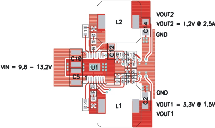
 Figure 24. Top Layer
 Figure 25. Bottom Layer
11.3 Overtemperature Protection and Junction Temperature Rise
The overtemperature thermal protection limits the maximum power to be dissipated at a given operating ambient temperature. In other words, at a given device power dissipation, the maximum ambient operating temperature is limited by the maximum allowable junction operating temperature. The device junction temperature is a function of power dissipation, and the thermal impedance from the junction to the ambient. If the internal die temperature must reach the thermal shutdown level, the TPS5429x shuts off both PWMs and remain in this state until the die temperature drops below 125°C, at which time the device restarts.
The first step in determining the device junction temperature is to calculate the power dissipation. The power dissipation is dominated by the two switching MOSFETs and the BP internal regulator. The power dissipated by each MOSFET is composed of conduction losses and switching losses. The total conduction loss in the high-side and low-side MOSFETs for each channel is given by Equation 42.

where
- IO is the DC output current,
- ΔIO is the peak-to-peak ripple current in the inductor
Notice the impact of operating duty cycle on the result.
The switching loss for each channel is approximated by Equation 43.

where
- COSS(HS) is the output capacitance of the high-side MOSFET
- COSS(LS) is the output capacitance of the low-side MOSFET
- ƒS is the switching frequency
The total power dissipation is found by summing the power loss for both MOSFETs plus the loss in the internal regulator (see Equation 44).

The temperature rise of the device junction is dependent on the thermal impedance from junction to the mounting pad, plus the thermal impedance from the thermal pad to ambient. The thermal impedance from the thermal pad to ambient is dependent on the PCB layout (PowerPAD™ interface to the PCB, the exposed pad area) and airflow (if any; see 関連資料 for more information).
The operating junction temperature is shown in Equation 45.

where
- θTH is the thermal impedance
11.4 Power Derating
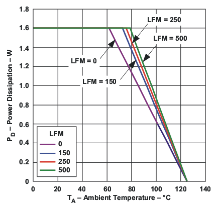
The TPS5429x delivers full current at wide duty cycles at ambient temperatures up to 85°C if the thermal impedance from the thermal pad is sufficient to maintain the junction temperature below the thermal shutdown level. At higher ambient temperatures, the device power dissipation must be reduced to maintain the junction temperature at or below the thermal shutdown level. Figure 26 illustrates the power derating for elevated ambient temperature under various air flow conditions. Note that these curves assume the PowerPAD™ is soldered to the recommended thermal pad. See 関連資料 for further information.
 Figure 26. Power Derating Curves