JAJSLH2 March   2021 TPS62810M , TPS62811M , TPS62812M , TPS62813M

PRODUCTION DATA  

  1. 特長
  2. アプリケーション
  3. 概要
  4. Revision History
  5. Device Comparison Table
  6. Pin Configuration and Functions
  7. Specifications
    1. 7.1 Absolute Maximum Ratings
    2. 7.2 ESD Ratings
    3. 7.3 Recommended Operating Conditions
    4. 7.4 Thermal Information
    5. 7.5 Electrical Characteristics
    6. 7.6 Typical Characteristics
  8. Parameter Measurement Information
    1. 8.1 Schematic
  9. Detailed Description
    1. 9.1 Overview
    2. 9.2 Functional Block Diagram
    3. 9.3 Feature Description
      1. 9.3.1 Precise Enable
      2. 9.3.2 COMP/FSET
      3. 9.3.3 MODE/SYNC
      4. 9.3.4 Spread Spectrum Clocking (SSC)
      5. 9.3.5 Undervoltage Lockout (UVLO)
      6. 9.3.6 Power Good Output (PG)
      7. 9.3.7 Thermal Shutdown
    4. 9.4 Device Functional Modes
      1. 9.4.1 Pulse Width Modulation (PWM) Operation
      2. 9.4.2 Power Save Mode Operation (PWM/PFM)
      3. 9.4.3 100% Duty-Cycle Operation
      4. 9.4.4 Current Limit and Short Circuit Protection
      5. 9.4.5 Foldback Current Limit and Short Circuit Protection
      6. 9.4.6 Output Discharge
      7. 9.4.7 Soft Start/Tracking (SS/TR)
  10. 10Application and Implementation
    1. 10.1 Application Information
      1. 10.1.1 Programming the Output Voltage
      2. 10.1.2 Inductor Selection
      3. 10.1.3 Capacitor Selection
        1. 10.1.3.1 Input Capacitor
        2. 10.1.3.2 Output Capacitor
    2. 10.2 Typical Application
      1. 10.2.1 Design Requirements
      2. 10.2.2 Detailed Design Procedure
      3. 10.2.3 Application Curves
    3. 10.3 System Examples
      1. 10.3.1 Voltage Tracking
      2. 10.3.2 Synchronizing to an External Clock
  11. 11Power Supply Recommendations
  12. 12Layout
    1. 12.1 Layout Guidelines
    2. 12.2 Layout Example
  13. 13Device and Documentation Support
    1. 13.1 Device Support
      1. 13.1.1 Third-Party Products Disclaimer
    2. 13.2 Documentation Support
      1. 13.2.1 Related Documentation
    3. 13.3 Receiving Notification of Documentation Updates
    4. 13.4 サポート・リソース
    5. 13.5 Trademarks
    6. 13.6 静電気放電に関する注意事項
    7. 13.7 用語集
  14. 14Mechanical, Packaging, and Orderable Information

パッケージ・オプション

メカニカル・データ(パッケージ|ピン)
サーマルパッド・メカニカル・データ
発注情報

Synchronizing to an External Clock

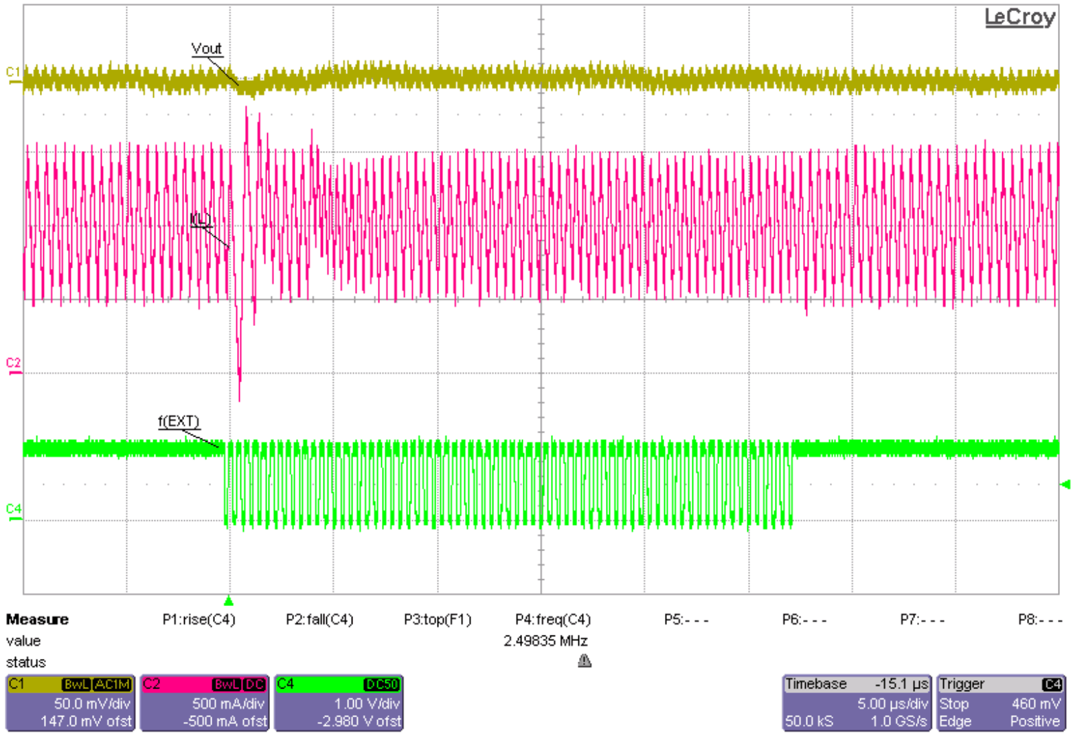
The TPS6281xM device can be externally synchronized by applying an external clock on the MODE/SYNC pin. There is no need for any additional circuitry as long as the input signal meets the requirements given in the electrical specifications. The clock can be applied or removed during operation, letting the user switch from an externally defined fixed frequency to power save mode or to an internally fixed-frequency operation. The value of the RCF resistor must be chosen so that the internally defined frequency and the externally applied frequency are close to each other. This ensures a smooth transition from internal to external frequency and vice versa.
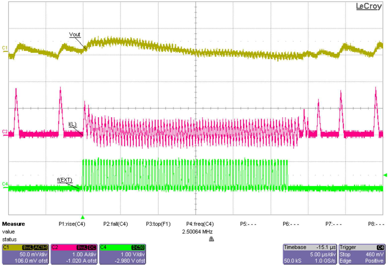
Figure 10-59 Schematic Using External Synchronization
GUID-4775287E-A021-4B87-B96C-1E0DD0998CA4-low.gif
VIN = 5 V RCF = 8.06 kΩ IOUT = 0.1 A
VOUT = 1.8 V fEXT = 2.5 MHz
Figure 10-60 Switching from External Syncronization to Power-Save Mode (PFM)
GUID-3DF7E2A5-F81E-4E6B-8471-4EE93B0AD606-low.gif
VIN = 5 V RCF = 8.06 kΩ IOUT = 1 A
VOUT = 1.8 V fEXT = 2.5 MHz
Figure 10-61 Switching from External Synchronization to Internal Fixed Frequency