JAJSJ61K
May 2020 – June 2024
TPS628501-Q1
,
TPS628502-Q1
,
TPS628503-Q1
PRODMIX
1
1
特長
2
アプリケーション
3
概要
4
Device Comparison Table
5
Pin Configuration and Functions
6
Specifications
6.1
Absolute Maximum Ratings
6.2
ESD Ratings
6.3
Recommended Operating Conditions
6.4
Thermal Information
6.5
Electrical Characteristics
6.6
Typical Characteristics
7
Parameter Measurement Information
7.1
Schematic
8
Detailed Description
8.1
Overview
8.2
Functional Block Diagram
8.3
Feature Description
8.3.1
Precise Enable (EN)
8.3.2
COMP/FSET
8.3.3
MODE / SYNC
8.3.4
Spread Spectrum Clocking (SSC)
8.3.5
Undervoltage Lockout (UVLO)
8.3.6
Power-Good Output (PG)
8.3.7
Thermal Shutdown
8.4
Device Functional Modes
8.4.1
Pulse Width Modulation (PWM) Operation
8.4.2
Power Save Mode Operation (PWM/PFM)
8.4.3
100% Duty-Cycle Operation
8.4.4
Current Limit and Short Circuit Protection
8.4.5
Foldback Current Limit and Short-Circuit Protection
8.4.6
Output Discharge
8.4.7
Input Overvoltage Protection
9
Application and Implementation
9.1
Application Information
9.1.1
Programming the Output Voltage
9.1.2
External Component Selection
9.1.2.1
Inductor Selection
9.1.3
Capacitor Selection
9.1.3.1
Input Capacitor
9.1.3.2
Output Capacitor
9.2
Typical Application
9.2.1
Design Requirements
9.2.2
Detailed Design Procedure
9.2.3
Application Curves
9.3
System Examples
9.3.1
Fixed Output Voltage Versions
9.3.2
Synchronizing to an External Clock
9.4
Power Supply Recommendations
9.5
Layout
9.5.1
Layout Guidelines
9.5.2
Layout Example
10
Device and Documentation Support
10.1
Device Support
10.1.1
サード・パーティ製品に関する免責事項
10.2
ドキュメントの更新通知を受け取る方法
10.3
サポート・リソース
10.4
Trademarks
10.5
静電気放電に関する注意事項
10.6
用語集
11
Revision History
12
Mechanical, Packaging, and Orderable Information
パッケージ・オプション
メカニカル・データ(パッケージ|ピン)
DRL|8
MPCS002E
サーマルパッド・メカニカル・データ
発注情報
jajsj61k_oa
jajsj61k_pm
6.6
Typical Characteristics
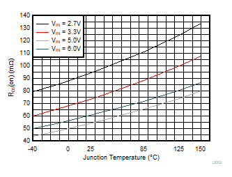
Figure 6-1
R
DS(ON)
of High-Side Switch
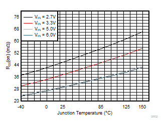
Figure 6-2
R
DS(ON)
of Low-Side Switch