JAJSJ23F September   2019  – October 2023 TPS62860 , TPS62861

PRODUCTION DATA  

  1.   1
  2. 特長
  3. アプリケーション
  4. 概要
  5. Revision History
  6. Device Comparison Table
  7. Pin Configuration and Functions
  8. Specifications
    1. 7.1 Absolute Maximum Ratings
    2. 7.2 ESD Ratings
    3. 7.3 Recommended Operating Conditions
    4. 7.4 Thermal Information
    5. 7.5 Electrical Characteristics
    6. 7.6 I2C Interface Timing Characteristics
    7. 7.7 Typical Characteristics
  9. Detailed Description
    1. 8.1 Overview
    2. 8.2 Functional Block Diagram
    3. 8.3 Feature Description
      1. 8.3.1  Power Save Mode
      2. 8.3.2  Forced PWM Operation
      3. 8.3.3  Smart Enable and Shutdown (EN)
      4. 8.3.4  Soft Start
      5. 8.3.5  Output Voltage Selection (VSEL) for TPS62860x
      6. 8.3.6  Output Voltage Selection (VSEL and I2C)
      7. 8.3.7  Forced PWM Mode During Output Voltage Change
      8. 8.3.8  Undervoltage Lockout (UVLO)
      9. 8.3.9  Power Good (PG)
      10. 8.3.10 Switch Current Limit and Short Circuit Protection
      11. 8.3.11 Thermal Shutdown
      12. 8.3.12 Output Voltage Discharge
    4. 8.4 Programming
      1. 8.4.1 Serial Interface Description
      2. 8.4.2 Standard- and Fast-Mode Protocol
      3. 8.4.3 I2C Update Sequence
      4. 8.4.4 I2C Register Reset
    5. 8.5 Register Map
      1. 8.5.1 Slave Address Byte
      2. 8.5.2 Register Address Byte
      3. 8.5.3 VOUT Register 1
      4. 8.5.4 VOUT Register 2
      5. 8.5.5 CONTROL Register
      6. 8.5.6 STATUS Register
  10. Application and Implementation
    1. 9.1 Application Information
    2. 9.2 Typical Application, TPS628610
      1. 9.2.1 Design Requirements
      2. 9.2.2 Detailed Design Procedure
        1. 9.2.2.1 Inductor Selection
        2. 9.2.2.2 Output Capacitor Selection
        3. 9.2.2.3 Input Capacitor Selection
      3. 9.2.3 Application Curves
    3. 9.3 Typical Application, TPS628600, TPS62860x
      1. 9.3.1 Design Requirements
      2. 9.3.2 Detailed Design Procedure
      3. 9.3.3 Application Curves
    4. 9.4 Power Supply Recommendations
    5. 9.5 Layout
      1. 9.5.1 Layout Guidelines
      2. 9.5.2 Layout Example
  11. 10Device and Documentation Support
    1. 10.1 Device Support
      1. 10.1.1 サード・パーティ製品に関する免責事項
    2. 10.2 ドキュメントの更新通知を受け取る方法
    3. 10.3 サポート・リソース
    4. 10.4 Trademarks
    5. 10.5 静電気放電に関する注意事項
    6. 10.6 用語集
  12. 11Mechanical, Packaging, and Orderable Information

パッケージ・オプション

メカニカル・データ(パッケージ|ピン)
サーマルパッド・メカニカル・データ
発注情報

Application Curves

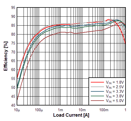
VIN = 3.8 V, VOUT = 1.1 V, TA = 25°C, unless otherwise noted
GUID-F645E888-9160-416D-A174-69FB62C9FAF2-low.gif
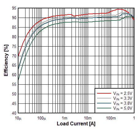
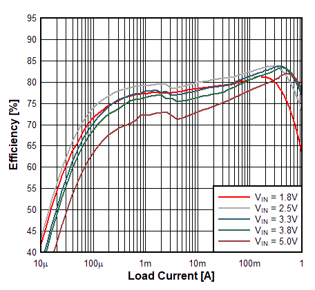
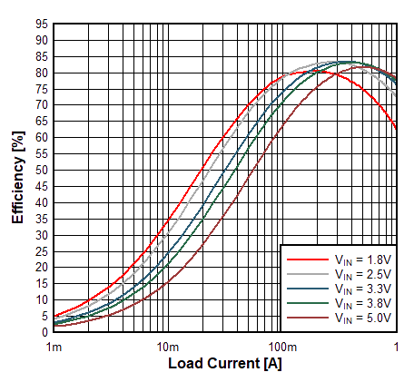
VOUT = 1.1 V Auto Power Save Mode
Figure 9-2 Efficiency
GUID-6EECC90A-A47B-4521-9284-762AE4E3036E-low.gif
VOUT = 1.9875 V Auto Power Save Mode
Figure 9-4 Efficiency
GUID-19A85684-DC64-4B1E-A4A6-C2659EF25572-low.gif
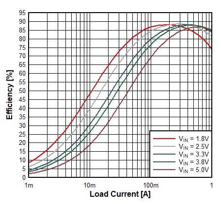
VOUT = 1.1 V Forced PWM Operation
Figure 9-6 Efficiency, Inductor Comparison
GUID-0F572790-A395-4524-A0B8-ED9C669F9B9D-low.gif
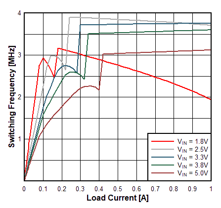
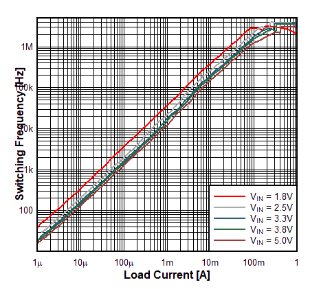
VOUT = 1.1 V Auto Power Save Mode
Figure 9-8 Switching Frequency
GUID-41AB67D9-9B77-4E8F-B8EF-A61AC36FF4ED-low.gif
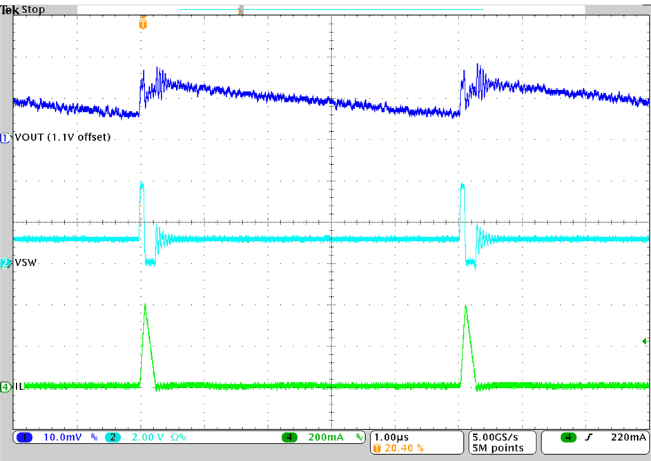
VSEL = HIGH
Figure 9-10 PFM Mode Operation
GUID-73E1C6F5-D265-4077-B72D-FC791681F9EF-low.gif
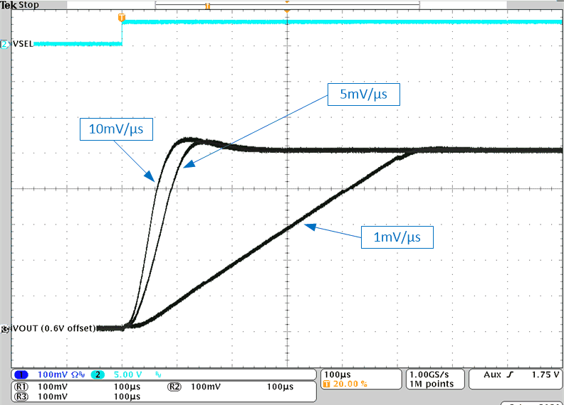
Default voltage setting
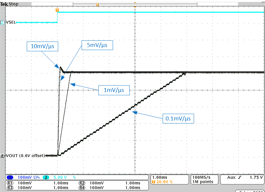
Figure 9-12 DVS by VSEL, Different Ramp Speed Settings
GUID-4E1B7202-3C74-4730-9E70-2E28D4CBC6AD-low.gif
Power Save Mode is active
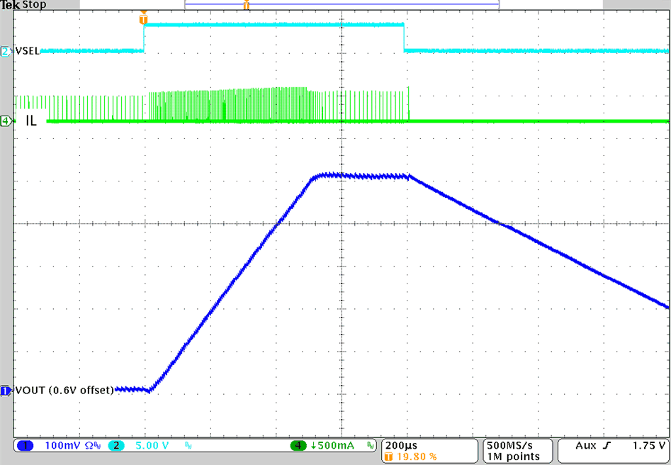
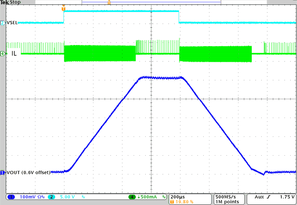
Figure 9-14 Standard Operation: VOUT Change
GUID-156F5876-AC20-45F6-8520-BD62AC5FB92E-low.gif
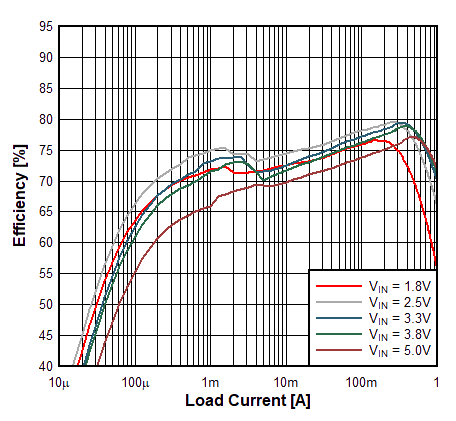
VOUT = 0.6 V Auto Power Save Mode
Figure 9-3 Efficiency
GUID-5105C89D-3CD8-4472-8AC6-6A4919B8DD77-low.gif
VOUT = 0.4 V Auto Power Save Mode
Figure 9-5 Efficiency
GUID-255D5D91-47EA-4069-ABF9-7E9298671E98-low.gif
VOUT = 0.6 V Forced PWM operation
Figure 9-7 Efficiency
GUID-92284F25-0956-4D0F-ACD7-23FAD96658E3-low.gif
VOUT = 1.1 V
Figure 9-9 Switching Frequency
GUID-850413CD-A5B0-4AB7-84BD-B567CB5C0305-low.gif
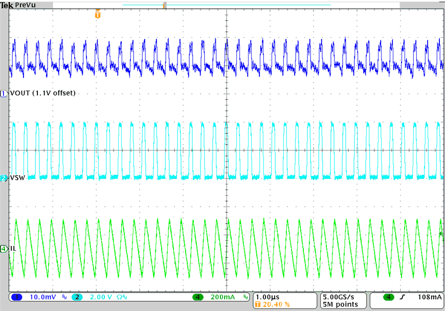
IOUT = 500 mA VSEL = HIGH
Figure 9-11 PWM-Mode Operation
GUID-BE3D45B6-51D2-4F76-8F52-7B2DBC8374E7-low.gif
Default voltage setting
Figure 9-13 DVS by VSEL, Different Ramp Speed Settings
GUID-46892E96-CA71-454E-B47C-2A2CA9D9BB93-low.gif
Power Save Mode is active
Figure 9-15 FPWM-Mode During VOUT Change Enabled