JAJSMS4F August 2021 – March 2024 TPS7H2211-SEP , TPS7H2211-SP
PRODUCTION DATA
- 1
- 1 特長
- 2 アプリケーション
- 3 概要
- 4 Device Options
- 5 Related Products
- 6 Pin Configuration and Functions
-
7 Specifications
- 7.1 Absolute Maximum Ratings
- 7.2 ESD Ratings
- 7.3 Recommended Operating Conditions
- 7.4 Thermal Information
- 7.5 Electrical Characteristics: All Devices
- 7.6 Electrical Characteristics: CFP and KGD Options
- 7.7 Electrical Characteristics: HTSSOP Option
- 7.8 Switching Characteristics: All Devices
- 7.9 Quality Conformance Inspection
- 7.10 Typical Characteristics
- 8 Parameter Measurement Information
- 9 Detailed Description
- 10Application and Implementation
- 11Device and Documentation Support
- 12Revision History
- 13Mechanical, Packaging, and Orderable Information
パッケージ・オプション
デバイスごとのパッケージ図は、PDF版データシートをご参照ください。
メカニカル・データ(パッケージ|ピン)
- DAP|32
- KGD|0
- HKR|16
サーマルパッド・メカニカル・データ
- DAP|32
発注情報
8 Parameter Measurement Information
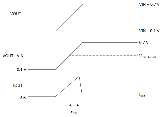
A. VIN is held constant during the test.
B. VRCP_ENTER is referenced from VOUT to VIN. It is the
threshold that, when reached, will turn-off the main switch FETs to prevent
reverse current flow.
Figure 8-1 Reverse Current Protection
Enter (VRCP_ENTER) Test Waveforms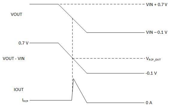
A. VIN is held constant during the test.
B. VRCP_EXIT is referenced from VOUT to VIN. It is the
threshold that, when reached, will turn-off the reverse current protection
feature.
Figure 8-2 Reverse Current Protection
Exit (VRCP_EXIT) Test Waveforms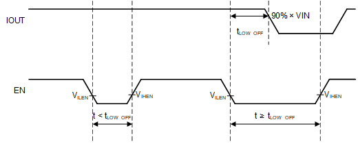 Figure 8-3 EN Signal Low Time to
Restart Device (tLOW_OFF)
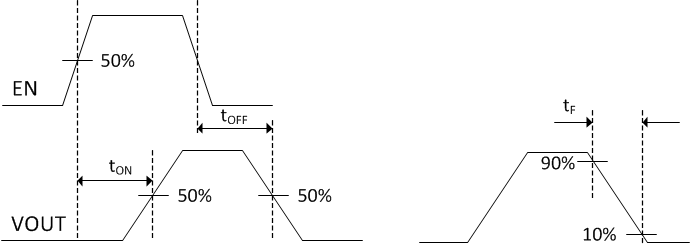 Figure 8-4 Turn-On Time (tON), Turn-Off Time (tOFF), and VOUT
Fall Time (tF) Waveforms
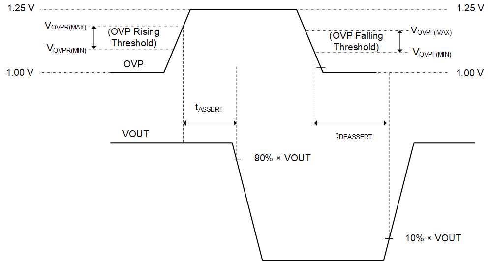
A. The OVP test signal uses a
typical rise time and fall time of 30 ns.
Figure 8-5 OVP Assert
(tASSERT) and OVP Deassert (tDEASSERT)
Waveforms