JAJSP14F August 1995 – August 2022 UC1823A , UC1825A , UC2823A , UC2823B , UC2825A , UC2825B , UC3823A , UC3823B , UC3825A , UC3825B
PRODUCTION DATA
- 1特長
- 2概要
- 3Revision History
- 4Ordering Information
- 5Pin Configuration and Functions
- 6Specifications
- 7Application and Implementation
- 8Device and Documentation Support
- 9Mechanical, Packaging, and Orderable Information
パッケージ・オプション
デバイスごとのパッケージ図は、PDF版データシートをご参照ください。
メカニカル・データ(パッケージ|ピン)
- N|16
- DW|16
サーマルパッド・メカニカル・データ
発注情報
7.6 HIGH CURRENT OUTPUTS
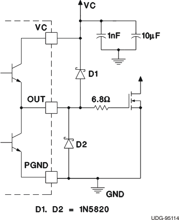
Each totem pole output of the UC3823A and UC3823AB, UC3825A, and UC3825B can deliver a 2-A peak current into a capacitive load. The output can slew a 1000-pF capacitor by 15 V in approximately 20 ns. Separate collector supply (VC) and power ground (PGND) pins help decouple the device's analog circuitry from the high-power gate drive noise. The use of 3-A Schottky diodes (1N5120, USD245, or equivalent) as shown in the Figure 7-10 from each output to both VC and PGND are recommended. The diodes clamp the output swing to the supply rails, necessary with any type of inductive/capacitive load, typical of a MOSFET gate. Schottky diodes must be used because a low forward voltage drop is required. DO NOT USE standard silicon diodes.
Although they are single-ended devices, two output drivers are available on the UC3823A and UC3823B devices. These can be paralleled by the use of a 0.5 Ω (noninductive) resistor connected in series with each output for a combined peak current of 4 A.
 Figure 7-9 Power MOSFET Drive Circuit