JAJSHM6E june 2019 – february 2021 UCC256402 , UCC256403 , UCC256404
PRODUCTION DATA
- 1
- 1 特長
- 2 アプリケーション
- 3 概要
- 4 Revision History
- Device Comparison Table
- 5 Pin Configuration and Functions
- 6 Specifications
-
7 Detailed Description
- 7.1 Overview
- 7.2 Functional Block Diagram
- 7.3 Feature Description
- 7.4 Device Functional Modes
-
Application and Implementation
- 8.1 Application Information
- 8.2
Typical Application
- 8.2.1 Design Requirements
- 8.2.2
Detailed Design Procedure
- 8.2.2.1 LLC Power Stage Requirements
- 8.2.2.2 LLC Gain Range
- 8.2.2.3 Select Ln and Qe
- 8.2.2.4 Determine Equivalent Load Resistance
- 8.2.2.5 Determine Component Parameters for LLC Resonant Circuit
- 8.2.2.6 LLC Primary-Side Currents
- 8.2.2.7 LLC Secondary-Side Currents
- 8.2.2.8 LLC Transformer
- 8.2.2.9 LLC Resonant Inductor
- 8.2.2.10 LLC Resonant Capacitor
- 8.2.2.11 LLC Primary-Side MOSFETs
- 8.2.2.12 LLC Rectifier Diodes
- 8.2.2.13 LLC Output Capacitors
- 8.2.2.14 HV Pin Series Resistors
- 8.2.2.15 BLK Pin Voltage Divider
- 8.2.2.16 ISNS Pin Differentiator
- 8.2.2.17 VCR Pin Capacitor Divider
- 8.2.2.18 BW Pin Voltage Divider
- 8.2.2.19 Soft Start and Burst Mode Programming
- 8.2.3 Application Curves
- 8 Power Supply Recommendations
- 9 Layout
- 10Device and Documentation Support
- Mechanical, Packaging, and Orderable Information
7.4.3 Burst Mode Control
The efficiency of an LLC converter power stage drops rapidly with falling output power. To maintain reasonable light load efficiency it is necessary to operate the LLC converter in burst mode. In this mode the LLC converter operates at relatively high power for a short burst period and then switching is stopped for a time period. During the burst period excess charge is transferred to and stored in the output capacitor. During the burst off period this stored charge is used to supply the load current. The burst mode operation is critical to meet strict standby power consumption requirements. But a challenge with burst mode operation is the audible noise performance. Due to the need to stop switching for certain time, there will be a pattern of switching pulses with frequencies that fall within the audible frequency range from 20 Hz to 20 kHz. Some device variants of UCC25640x includes a burst mode with soft on and soft off periods at the first few and last few switching pulses, minimizing the audible noise during standby operation.
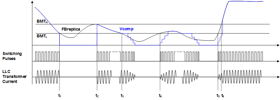
Figure 7-17 describes the timing diagram of the burst mode operation. Two burst mode thresholds are used (BMTH for burst mode exit and BMTL for burst mode entry). The details of how to program these two thresholds are described in Section 7.4.3.1 section. The FBreplica from the FB chain is compared with the two thresholds, and determines the burst mode operation.
- At t1, FBreplica is below BMTL. The system enters burst mode and stops switching immediately. During the burst off period, UCC25640x disables some internal blocks to save power consumption.
- At t2, FBreplica is above BMTH. The system starts to switch again, and this period is referred to as the burst on period. During burst on period, the control effort Vcomp sent to the VCR comparator is the higher value of FBreplica and BMTL. For the first switching pattern after the system enters burst mode, there is no burst soft on.
- At t3, FBreplica falls below BMTL again. Switching will not stop until it reaches the predefined number (Nburst) of a burst packet. The Vcomp still selects the higher value of FBreplica and BMTL. For the last 7 switching cycles, soft off will be applied (only 3 soft on/off steps are shown in Figure 7-17 for conceptual introduction). The Vcomp is a fraction of the higher value between FBreplica and BMTL. The number of fractions for different switching cycles are described in Table 7-1. For burst soft off, it starts from step 7 and ramps down. After it reaches step 1, soft off steps are completed and the system enters burst off period. This helps to achieve slow ramping down of the LLC transformer current. For burst soft on, it reverses the direction by starting from step 1 and ends at step 7. If FBreplica becomes greater than BMTL before the soft off steps are completed, the burst soft off will end immediately and the system transitions to burst soft on. In this condition, the soft on step starts from the step where soft off ends at, to ensure a smooth transition between soft off and soft on.
- At t4, FBreplica is greater than BMTL. The system enters burst on period, and since this is not the first burst on period, there is soft on period at the first 7 switching cycles. The fraction of Vcomp to the higher value of FBreplica and BMTL is also described in Table 7-1. After burst soft on steps are completed, Vcomp uses the higher value of FBreplia and BMTL until it reaches burst soft off periods.
- At t5, FBreplica is greater than BMTL again after another burst off period. This time the difference is that FBreplica is greater than BMTH at t6, when the burst soft on steps are not completed yet. The burst soft on will get terminated immediately, so that Vcomp can follow the FBreplica. This is to ensure a quick system response during a load transient from burst mode operation to out-of-burst mode operation.
 Figure 7-17 Burst Mode Switching Pattern
| Burst Soft On and Soft Off Step | Fraction used for Reduced Vcomp During Soft On |
|---|---|
| 1 | 1/3 |
| 2 | 9/21 |
| 3 | 11/21 |
| 4 | 13/21 |
| 5 | 15/21 |
| 6 | 17/21 |
| 7 | 19/21 |
The HHC control makes the implementation of the burst soft on and soft off very straight forward. Due to the frequency control portion in HHC, changing the Vcomp can directly impact the LLC switching frequency to control the resonant current magnitude within switching cycles. Also the last pulse of each burst on period is turned off when the VCR node voltage equals the common mode voltage VCM. In HHC control, this is approximately equivalent to resonant capacitor voltage equal to VIN/2. This operation keeps the resonant capacitor voltage to approximate VIN/2 for each burst off period, thus enabling the burst pattern to settle as soon as possible during the burst on period.
As described in Section 7.3.9.1, in order to avoid nuisance ZCS detection at light load condition, ZCS is disabled at light load condition. This is achieved by using the BMTH threshold. When FBreplica is below BMTH, indicating a light load operating condition, ZCS detection is disabled. When FBreplica is above BMTH, ZCS detection will resume.
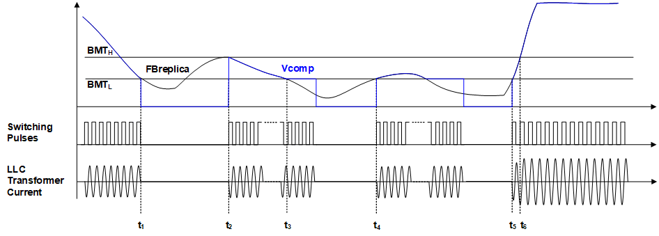
Some device variants disables the burst soft on and soft off feature, for applications that have less concern about audible noise, but want smaller output ripple during burst mode. A smaller burst packet size is also used. The timing diagram of the burst mode operation for when burst soft on and soft off is disabled is described in Figure 7-18.
- At t1, FBreplica is below BMTL. The system enters burst mode and stops switching immediately.
- At t2, FBreplica is above BMTH. The system starts to switch again, and enters burst on period. The control effort Vcomp sent to the VCR comparator is the higher value of FBreplica and BMTL.
- At t3, FBreplica falls below BMTL again. Switching will not stop until it reaches the predefined number (Nburst) of a burst packet. If switching reaches the Nburst before FBreplica falls below BMTL again, system will continue to deliver burst packet until FBreplica is below BMTL.
- At t4, FBreplica is greater than BMTL. The system enters burst on period without soft on. So the control effort Vcomp is the higher value of FBreplica and BMTL.
- At t5, FBreplica is greater than BMTL again after another burst off period. The control effort Vcomp follows FBreplica. At t6, FBreplica becomes above BMTH, Vcomp still follows FBreplica. If FBreplica remains above BMTH more than Nburst switching cycles, system exits burst mode.
 Figure 7-18 Burst Mode Switching Pattern when Soft On and Soft Off is Disabled
UCC25640x can also disable the burst mode by changing the BW pin resistance, as described in Section 7.4.3.2. When burst mode is disabled, the switching does not stop even when FBreplica becomes lower than BMTL. The pick higher block still works by picking the higher value of BMTL and FBreplica for the control effort Vcomp. In this case, BMTL will limit the maximum switching frequency of LLC.
When burst mode is disabled, FBreplica needs to be higher than BMTL at steady state. Otherwise, LLC output voltage will lose regulation as it continues deliver more energy than what is demanded from the feedback. For a transient period, it is ok for FBreplica to be lower than BMTL.