SGLS121D December 2002 – June 2020 UCC2800-Q1 , UCC2801-Q1 , UCC2802-Q1 , UCC2803-Q1 , UCC2804-Q1 , UCC2805-Q1
PRODUCTION DATA.
- 1 Features
- 2 Applications
- 3 Description
- 4 Revision History
- 5 Description (continued)
- 6 Device Comparison Table
- 7 Pin Configuration and Functions
- 8 Specifications
-
9 Detailed Description
- 9.1 Overview
- 9.2 Functional Block Diagram
- 9.3
Feature Description
- 9.3.1 Detailed Pin Description
- 9.3.2 Undervoltage Lockout (UVLO)
- 9.3.3 Self-Biasing, Active Low Output
- 9.3.4 Reference Voltage
- 9.3.5 Oscillator
- 9.3.6 Synchronization
- 9.3.7 PWM Generator
- 9.3.8 Minimum Off-Time Setting (Dead-Time Control)
- 9.3.9 Leading Edge Blanking
- 9.3.10 Minimum Pulse Width
- 9.3.11 Current Limiting
- 9.3.12 Overcurrent Protection and Full Cycle Restart
- 9.3.13 Soft Start
- 9.3.14 Slope Compensation
- 9.4 Device Functional Modes
- 10Application and Implementation
- 11Power Supply Recommendations
- 12Layout
- 13Device and Documentation Support
- 14Mechanical, Packaging, and Orderable Information
パッケージ・オプション
デバイスごとのパッケージ図は、PDF版データシートをご参照ください。
メカニカル・データ(パッケージ|ピン)
- D|8
サーマルパッド・メカニカル・データ
発注情報
9.3.2 Undervoltage Lockout (UVLO)
The UCC280x-Q1 devices feature undervoltage lockout protection circuits for controlled operation during power-up and power-down sequences. Both the supply voltage (VCC) and the reference voltage (Vref) are monitored by the UVLO circuitry. An active low, self-biasing totem pole output during UVLO design is also incorporated for enhanced power switch protection.
Undervoltage lockout thresholds for the UCC2802-Q1, UCC2803-Q1, UCC2804-Q1, and UCC2805-Q1 devices are different from the previous generation of UCx842-Q1, UCx843-Q1, UCx844-Q1, and UCx845-Q1 PWMs. Basically, the thresholds are optimized for two groups of applications: off-line power supplies and DC-DC converters.
The UCC2802-Q1 and UCC2804-Q1 feature typical UVLO thresholds of 12.5 V for turnon and 8.3 V for turnoff, providing 4.3 V of hysteresis.
For low voltage inputs, which include battery and 5-V applications, the UCC2803-Q1 and UCC2805-Q1 turn on at 4.1 V and turn off at 3.6 V with 0.5 V of hysteresis.
The UCC2800-Q1 and UCC2801-Q1 have UVLO thresholds optimized for automotive and battery applications.
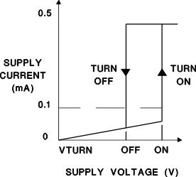
During UVLO the IC draws approximately 100 μA of supply current. Once crossing the turnon threshold the IC supply current increases typically to about 500 μA, over an order of magnitude lower than bipolar counterparts.
 Figure 11. IC Supply Current at UVLO
 Table 1. UVLO Level Comparison Table
| DEVICE | Vton (V) | Vtoff (V) |
|---|---|---|
| UCC2800-Q1 | 7.2 | 6.9 |
| UCC2801-Q1 | 9.4 | 7.4 |
| UCC2802-Q1, UCC2804-Q1 | 12.5 | 8.3 |
| UCC2803-Q1, UCC2805-Q1 | 4.1 | 3.6 |