JAJSCJ6C September 2016 – October 2024 UCC28950-Q1 , UCC28951-Q1
PRODUCTION DATA
- 1
- 1 特長
- 2 アプリケーション
- 3 概要
- 4 Pin Configuration and Functions
- 5 Specifications
-
6 Detailed Description
- 6.1 Overview
- 6.2 Functional Block Diagram
- 6.3
Feature Description
- 6.3.1 Start-Up Protection Logic
- 6.3.2 Voltage Reference (VREF)
- 6.3.3 Error Amplifier (EA+, EA–, COMP)
- 6.3.4 Soft-Start and Enable (SS/EN)
- 6.3.5 Light-Load Power Saving Features
- 6.3.6 Adaptive Delay, (Delay Between OUTA and OUTB, OUTC and OUTD (DELAB, DELCD, ADEL))
- 6.3.7 Adaptive Delay (Delay Between OUTA and OUTF, OUTB and OUTE (DELEF, ADELEF)
- 6.3.8 Minimum Pulse (TMIN)
- 6.3.9 Burst Mode
- 6.3.10 Switching Frequency Setting
- 6.3.11 Slope Compensation (RSUM)
- 6.3.12 Dynamic SR ON/OFF Control (DCM Mode)
- 6.3.13 Current Sensing (CS)
- 6.3.14 Cycle-by-Cycle Current Limit Current Protection and Hiccup Mode
- 6.3.15 Synchronization (SYNC)
- 6.3.16 Outputs (OUTA, OUTB, OUTC, OUTD, OUTE, OUTF)
- 6.3.17 Supply Voltage (VDD)
- 6.3.18 Ground (GND)
- 6.4 Device Functional Modes
-
7 Application and Implementation
- 7.1 Application Information
- 7.2
Typical Application
- 7.2.1 Design Requirements
- 7.2.2
Detailed Design Procedure
- 7.2.2.1 Power Loss Budget
- 7.2.2.2 Preliminary Transformer Calculations (T1)
- 7.2.2.3 QA, QB, QC, QD FET Selection
- 7.2.2.4 Selecting LS
- 7.2.2.5 Selecting Diodes DB and DC
- 7.2.2.6 Output Inductor Selection (LOUT)
- 7.2.2.7 Output Capacitance (COUT)
- 7.2.2.8 Select FETs QE and QF
- 7.2.2.9 Input Capacitance (CIN)
- 7.2.2.10 Current Sense Network (CT, RCS, R7, DA)
- 7.2.3 Application Curves
- 7.3 Power Supply Recommendations
- 7.4 Layout
- 8 Device and Documentation Support
- 9 Revision History
- 10Mechanical, Packaging, and Orderable Information
7.2.3 Application Curves
Switch node QBd is valley switching and node QDd has achieved ZVS. Please refer to Figure 7-13 and Figure 7-14. It is not uncommon for switch node QDd to obtain ZVS before QBd. This is because during the QDd switch node voltage transition, the reflected output current provides immediate energy for the LC tank at the switch node. Where at the QBd switch node transition the primary has been shorted out by the high-side or low-side FETs in the H bridge. This transition is dependent on the energy stored in LS and LLK to provide energy for the LC tank at switch node QBd making it take longer to achieve ZVS.
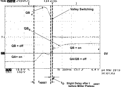
| VIN = 390V | IOUT = 5A |
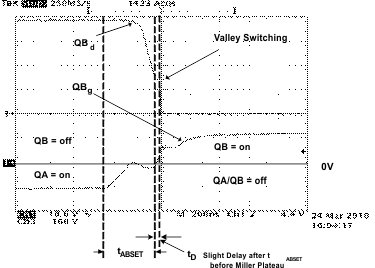
| VIN = 390V | IOUT = 10A |
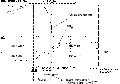
| VIN = 390V | IOUT = 5A |
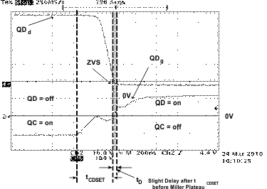
| VIN = 390V | IOUT = 10A |
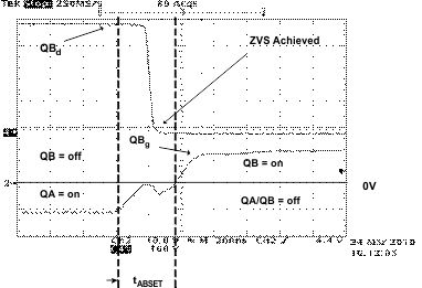
| VIN = 390V | IOUT = 25A |
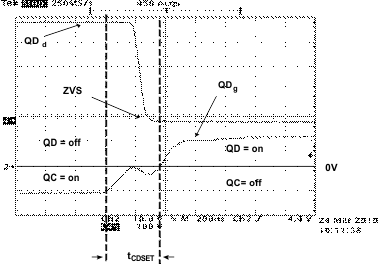
| VIN = 390V | IOUT = 25A |
When the converter is running at 25A, both switch nodes are operating into zero voltage switching (ZVS). It is also worth mentioning that there is no evidence of the gate miller plateau during gate driver switching. This is because the voltage across the drains and sources of FETs QA through QD transitioned earlier.
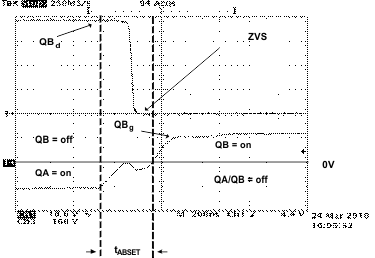
| VIN = 390V | IOUT = 50A |
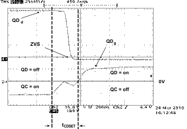
| VIN = 390V | IOUT = 50A |
| ZVS maintained from 50% to 100% output power |