SWRS152N June 2013 – April 2021 WL1801MOD , WL1805MOD , WL1831MOD , WL1835MOD
PRODUCTION DATA
- 1 Features
- 2 Applications
- 3 Description
- 4 Functional Block Diagram
- 5 Revision History
- 6 Device Comparison
- 7 Terminal Configuration and Functions
-
8 Specifications
- 8.1 Absolute Maximum Ratings
- 8.2 ESD Ratings
- 8.3 Recommended Operating Conditions
- 8.4 External Digital Slow Clock Requirements
- 8.5 Thermal Resistance Characteristics for MOC 100-Pin Package
- 8.6 WLAN Performance: 2.4-GHz Receiver Characteristics
- 8.7 WLAN Performance: 2.4-GHz Transmitter Power
- 8.8 WLAN Performance: Currents
- 8.9 Bluetooth Performance: BR, EDR Receiver Characteristics—In-Band Signals
- 8.10 Bluetooth Performance: Transmitter, BR
- 8.11 Bluetooth Performance: Transmitter, EDR
- 8.12 Bluetooth Performance: Modulation, BR
- 8.13 Bluetooth Performance: Modulation, EDR
- 8.14 Bluetooth low energy Performance: Receiver Characteristics – In-Band Signals
- 8.15 Bluetooth low energy Performance: Transmitter Characteristics
- 8.16 Bluetooth low energy Performance: Modulation Characteristics
- 8.17 Bluetooth BR and EDR Dynamic Currents
- 8.18 Bluetooth low energy Currents
- 8.19
Timing and Switching Characteristics
- 8.19.1 Power Management
- 8.19.2 Power-Up and Shut-Down States
- 8.19.3 Chip Top-level Power-Up Sequence
- 8.19.4 WLAN Power-Up Sequence
- 8.19.5 Bluetooth-Bluetooth low energy Power-Up Sequence
- 8.19.6 WLAN SDIO Transport Layer
- 8.19.7 HCI UART Shared-Transport Layers for All Functional Blocks (Except WLAN)
- 8.19.8 Bluetooth Codec-PCM (Audio) Timing Specifications
- 9 Detailed Description
- 10Applications, Implementation, and Layout
- 11Device and Documentation Support
- 12Mechanical, Packaging, and Orderable Information
パッケージ・オプション
デバイスごとのパッケージ図は、PDF版データシートをご参照ください。
メカニカル・データ(パッケージ|ピン)
- MOC|100
サーマルパッド・メカニカル・データ
発注情報
9 Detailed Description
The WiLink 8 module is a self-contained connectivity solution based on WiLink 8 connectivity. As the eighth-generation connectivity combo chip from TI, the WiLink 8 module is based on proven technology.
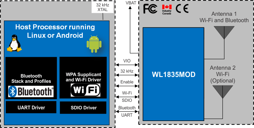
Figure 9-1 shows a high-level view of the WL1835MOD variant.
 Figure 9-1 WL1835MOD High-Level System Diagram
Table 9-1, Table 9-2, and Table 9-3 list performance parameters along with shutdown and sleep currents.
Table 9-1 WLAN Performance Parameters
| WLAN(1) | CONDITIONS | SPECIFICATION (TYP) | UNIT |
|---|---|---|---|
| Maximum TX power | 1-Mbps DSSS | 17.3 | dBm |
| Minimum sensitivity | 1-Mbps DSSS | –96.3 | dBm |
| Sleep current | Leakage, firmware retained | 160 | µA |
| Connected IDLE | No traffic IDLE connect | 750 | µA |
| RX search | Search (SISO20) | 54 | mA |
| RX current (SISO20) | MCS7, 2.4 GHz | 65 | mA |
| TX current (SISO20) | MCS7, 2.4 GHz, +11.2 dBm | 238 | mA |
| Maximum peak current consumption during calibration(2) | 850 | mA |
(1) System design power scheme must comply with both peak and average TX bursts.
(2) Peak current VBAT can hit 850 mA during device calibration.
- At wakeup, the WiLink 8 module performs the entire calibration sequence at the center of the 2.4-GHz band.
- After a link is established, calibration is performed periodically (every 5 minutes) on the specific channel tuned.
- The maximum VBAT value is based on peak calibration consumption with a 30% margin.
Table 9-2 Bluetooth Performance Parameters
| Bluetooth | CONDITIONS | SPECIFICATION (TYP) | UNIT |
|---|---|---|---|
| Maximum TX power | GFSK | 11.7 | dBm |
| Minimum sensitivity | GFSK | –92.2 | dBm |
| Sniff | 1 attempt, 1.28 s (+4 dBm) | 178 | µA |
| Page or inquiry | 1.28-s interrupt, 11.25-ms scan window (+4 dBm) | 253 | µA |
| A2DP | MP3 high quality 192 kbps (+4 dBm) | 7.5 | mA |
Table 9-3 Shutdown and Sleep Currents
| PARAMETER | POWER SUPPLY CURRENT | TYP | UNIT |
|---|---|---|---|
| Shutdown mode All functions shut down |
VBAT | 10 | µA |
| VIO | 2 | ||
| WLAN sleep mode | VBAT | 160 | µA |
| VIO | 60 | ||
| Bluetooth sleep mode | VBAT | 110 | µA |
| VIO | 60 |