JAJSAQ5F December 2007 – October 2016 DAC121C081 , DAC121C085
PRODUCTION DATA.
- 1 特長
- 2 アプリケーション
- 3 概要
- 4 改訂履歴
- 5 概要(続き)
- 6 Pin Configuration and Functions
- 7 Specifications
- 8 Detailed Description
- 9 Application and Implementation
- 10Power Supply Recommendations
- 11Layout
- 12デバイスおよびドキュメントのサポート
- 13メカニカル、パッケージ、および注文情報
6 Pin Configuration and Functions
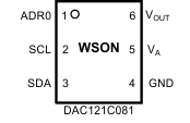
NGF Package
6-Pins WSON
Top View

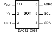
DDC Package
6-Pin SOT
Top View

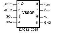
DGK Package
8-Pins VSSOP
Top View

Pin Functions
| PIN | TYPE | DESCRIPTION | EQUIVALENT CIRCUIT | |||
|---|---|---|---|---|---|---|
| NAME | WSON | SOT | VSSOP | |||
| ADR0 | 1 | 6 | 1 | Digital Input, three levels |
Tri-state Address Selection Input. Sets the two Least Significant Bits (A1 and A0) of the 7-bit slave address. (see Table 1) |
 |
| ADR1 | — | — | 2 | Digital Input, three levels |
Tri-state Address Selection Input. Sets Bits A6 and A3 of the 7-bit slave address. (see Table 1) | |
| GND | 4 | 3 | 5 | Ground | Ground for all on-chip circuitry | — |
| SCL | 2 | 5 | 3 | Digital Input | Serial Clock Input. SCL is used together with SDA to control the transfer of data in and out of the device. |
 |
| SDA | 3 | 4 | 4 | Digital Input/Output |
Serial Data bi-directional connection. Data is clocked into or out of the internal 16-bit register relative to the clock edges of SCL. This is an open-drain data line that must be pulled to the supply (VA) by an external pullup resistor. | |
| VOUT | 6 | 1 | 8 | Analog Output | Analog Output Voltage | — |
| VA | 5 | 2 | 6 | Supply | Power supply input. For the SOT and WSON versions, this supply is used as the reference. Must be decoupled to GND. | — |
| VREF | — | — | 7 | Supply | Unbufferred reference voltage. For the VSSOP, this supply is used as the reference. VREF must be free of noise and decoupled to GND. | — |
| PAD | (LLP only) | — | — | Ground | Exposed die attach pad can be connected to ground or left floating. Soldering the pad to the PCB offers optimal thermal performance and enhances package self-alignment during reflow. | — |