JAJSC24H June 2013 – November 2016 TPS65132 , TPS65132S
UNLESS OTHERWISE NOTED, this document contains PRODUCTION DATA.
- 1 特長
- 2 アプリケーション
- 3 概要
- 4 改訂履歴
- 5 Device Comparison Table
- 6 Pin Configuration and Functions
- 7 Specifications
- 8 Detailed Description
-
9 Application and Implementation
- 9.1 Application Information
- 9.2
Typical Applications
- 9.2.1
Low-current Applications (≤ 40 mA)
- 9.2.1.1 Design Requirements
- 9.2.1.2 Detailed Design Procedure
- 9.2.1.3 Application Curves
- 9.2.2
Mid-current Applications (≤ 80 mA)
- 9.2.2.1 Design Requirements
- 9.2.2.2 Detailed Design Procedure
- 9.2.2.3 Application Curves
- 9.2.3 High-current Applications (≤ 150 mA)
- 9.2.1
Low-current Applications (≤ 40 mA)
- 10Power Supply Recommendations
- 11Layout
- 12デバイスおよびドキュメントのサポート
- 13メカニカル、パッケージ、および注文情報
7 Specifications
7.1 Absolute Maximum Ratings(1)(2)
over operating free-air temperature range (unless otherwise noted)| VALUE | UNIT | |||
|---|---|---|---|---|
| MIN | MAX | |||
| Voltage range | CFLY1, EN, ENN, ENP, OUTP, REG, SCL, SDA, SW, SYNC, VIN | –0.3 | 7 | V |
| CFLY2, OUTN | –7 | 0.3 | V | |
| Continuous total power dissipation | See Thermal Information | |||
| Operating junction temperature, TJ | –40 | 150 | °C | |
| Operating ambient temperature, TA | –40 | 85 | °C | |
| Storage temperature, Tstg | –65 | 150 | °C | |
(1) Stresses beyond those listed under absolute maximum ratings may cause permanent damage to the device. These are stress ratings only, and functional operation of the device at these or any other conditions beyond those indicated under recommended operating conditions is not implied. Exposure to absolute–maximum–rated conditions for extended periods may affect device reliability.
(2) All voltage values are with respect to ground.
7.2 ESD Ratings
| VALUE | UNIT | |||
|---|---|---|---|---|
| VESD | Human body model (HBM), per ANSI/ESDA/JEDEC JS-001, all pins(1) | ±2000 | V | |
| Charged device model (CDM) per JEDEC specification JESD22-C101, all pins(2) | ±500 | V | ||
(1) JEDEC document JEP155 states that 500-V HBM allows safe manufacturing with a standard ESD control process.
(2) JEDEC document JEP157 states that 250-V CDM allows safe manufacturing with a standard ESD control process.
7.3 Recommended Operating Conditions
| MIN | TYP | MAX | UNIT | ||
|---|---|---|---|---|---|
| VIN | Input voltage range | 2.5 | 5.5 | V | |
| L | Inductor(1) | 2.2 | 4.7 | µH | |
| CIN | Input capacitor(1)(2) | 4.7 | µF | ||
| CFLY | Flying capacitor(1)(2) | 2.2 | µF | ||
| COUTP, COUTN, CREG | Output capacitors(1)(2) | 4.7 | µF | ||
| TA | Operating ambient temperature | –40 | 85 | °C | |
| TJ | Operating junction temperature | –40 | 125 | °C | |
(1) Please see Detailed Description section for further information.
(2) X7R (or better dielectric material) is recommended.
7.4 Thermal Information
| THERMAL METRIC(1) | TPS65132 | TPS65132 | UNIT | |
|---|---|---|---|---|
| YFF | RVC | |||
| (15) BALLS | (20) PINS | |||
| RθJA | Junction-to-ambient thermal resistance | 76.5 | 39.0 | °C/W |
| RθJCtop | Junction-to-case (top) thermal resistance | 0.2 | 42.7 | °C/W |
| RθJB | Junction-to-board thermal resistance | 44 | 13.6 | °C/W |
| ψJT | Junction-to-top characterization parameter | 1.6 | 0.6 | °C/W |
| ψJB | Junction-to-board characterization parameter | 43.4 | 13.6 | °C/W |
| RθJCbot | Junction-to-case (bottom) thermal resistance | N/A | 3.8 | °C/W |
(1) For more information about traditional and new thermal metrics, see the Semiconductor and IC Package Thermal Metrics application report, SPRA953.
7.5 Electrical Characteristics
VIN = 3.7 V, EN = ENN = ENP = VIN, VPOS = 5.4 V, VNEG = –5.4 V, TA = –40°C to 85°C; typical values are at TA = 25°C(unless otherwise noted).
7.6 I2C Interface Timing Requirements / Characteristics (1)
| PARAMETER | TEST CONDITIONS | MIN | TYP | MAX | UNIT | |
|---|---|---|---|---|---|---|
| fSCL | SCL clock frequency | Standard mode | 100 | kHz | ||
| Fast mode | 400 | kHz | ||||
| tLOW | LOW period of the SCL clock | Standard mode | 4.7 | µs | ||
| Fast mode | 1.3 | µs | ||||
| tHIGH | HIGH period of the SCL clock | Standard mode | 4.0 | µs | ||
| Fast mode | 600 | ns | ||||
| tBUF | Bus free time between a STOP and START condition | Standard mode | 4.7 | µs | ||
| Fast mode | 1.3 | µs | ||||
| thd;STA | Hold time for a repeated START condition | Standard mode | 4.0 | µs | ||
| Fast mode | 600 | ns | ||||
| tsu;STA | Setup time for a repeated START condition | Standard mode | 4.7 | µs | ||
| Fast mode | 600 | ns | ||||
| tsu;DAT | Data setup time | Standard mode | 250 | ns | ||
| Fast mode | 100 | ns | ||||
| thd;DAT | Data hold time | Standard mode | 0.05 | 3.45 | µs | |
| Fast mode | 0.05 | 0.9 | µs | |||
| tRCL1 | Rise time of SCL signal after a repeated START condition and after an acknowledge bit | Standard mode | 20 + 0.1CB | 1000 | ns | |
| Fast mode | 20 + 0.1CB | 1000 | ns | |||
| tRCL | Rise time of SCL signal | Standard mode | 20 + 0.1CB | 1000 | ns | |
| Fast mode | 20 + 0.1CB | 300 | ns | |||
| tFCL | Fall time of SCL signal | Standard mode | 20 + 0.1CB | 300 | ns | |
| Fast mode | 20 + 0.1CB | 300 | ns | |||
| tRDA | Rise time of SDA signal | Standard mode | 20 + 0.1CB | 1000 | ns | |
| Fast mode | 20 + 0.1CB | 300 | ns | |||
| tFDA | Fall time of SDA signal | Standard mode | 20 + 0.1CB | 300 | ns | |
| Fast mode | 20 + 0.1CB | 300 | ns | |||
| tsu;STO | Setup time for STOP condition | Standard mode | 4.0 | µs | ||
| Fast mode | 600 | ns | ||||
| CB | Capacitive load for SDA and SCL | 0.4 | nF | |||
(1) Industry standard I2C timing characteristics according to I2C-Bus Specification, Version 2.1, January 2000. Not tested in production.
 Figure 1. Serial Interface Timing For F/S-Mode
7.7 Typical Characteristics
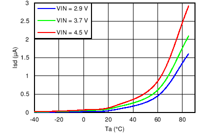
VIN= 3.7 V, VPOS= 5.4 V, VNEG= –5.4 V, unless otherwise noted Figure 2. Shutdown Current (all versions but Ax)
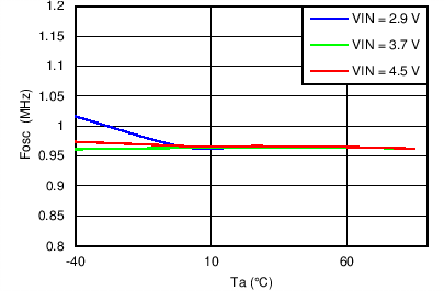
 Figure 4. Main Oscillator Frequency
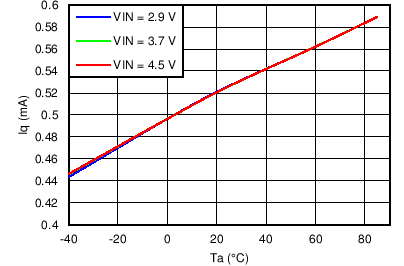
 Figure 3. Quiescent Current
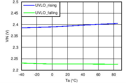
 Figure 5. UVLO