JAJSDM5E September 2017 – November 2019 TLV7011 , TLV7012 , TLV7021 , TLV7022
PRODUCTION DATA.
- 1 特長
- 2 アプリケーション
- 3 概要
- 4 改訂履歴
- 5 概要 (続き)
- 6 Pin Configuration and Functions
-
7 Specifications
- 7.1 Absolute Maximum Ratings (Single)
- 7.2 Absolute Maximum Ratings (Dual)
- 7.3 ESD Ratings
- 7.4 Recommended Operating Conditions (Single)
- 7.5 Recommended Operating Conditions (Dual)
- 7.6 Thermal Information (Single)
- 7.7 Thermal Information (Dual)
- 7.8 Electrical Characteristics (Single)
- 7.9 Switching Characteristics (Single)
- 7.10 Electrical Characteristics (Dual)
- 7.11 Switching Characteristics (Dual)
- 7.12 Timing Diagrams
- 7.13 Typical Characteristics
- 8 Detailed Description
- 9 Application and Implementation
- 10Power Supply Recommendations
- 11Layout
- 12デバイスおよびドキュメントのサポート
- 13メカニカル、パッケージ、および注文情報
6 Pin Configuration and Functions
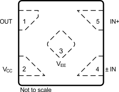
DPW Package
5-Pin X2SON
Top View

Pin Functions
| PIN | I/O/P(1) | DESCRIPTION | ||
|---|---|---|---|---|
| NAME | X2SON | SOT-23, SC70 | ||
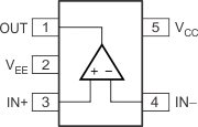
| OUT | 1 | 1 | O | Output |
| VCC | 2 | 5 | P | Positive (highest) power supply |
| VEE | 3 | 2 | P | Negative (lowest) power supply |
| IN– | 4 | 4 | I | Inverting input |
| IN+ | 5 | 3 | I | Noninverting input |
(1) I = Input, O = Output, P = Power
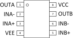
TLV7012/22 DGK Packages
8-Pin VSSOP
Top View

Pin Functions: TLV7012/22
| PIN | I/O | DESCRIPTION | |
|---|---|---|---|
| NAME | NO. | ||
| INA– | 2 | I | Inverting input, channel A |
| INA+ | 3 | I | Noninverting input, channel A |
| INB– | 6 | I | Inverting input, channel B |
| INB+ | 5 | I | Noninverting input, channel B |
| OUTA | 1 | O | Output, channel A |
| OUTB | 7 | O | Output, channel B |
| VEE | 4 | — | Negative (lowest) supply or ground (for single-supply operation) |
| VCC | 8 | — | Positive (highest) supply |
