JAJSDN1B April 2017 – December 2017 TPS22971
PRODUCTION DATA.
9 Application and Implementation
NOTE
Information in the following applications sections is not part of the TI component specification, and TI does not warrant its accuracy or completeness. TI’s customers are responsible for determining suitability of components for their purposes. Customers should validate and test their design implementation to confirm system functionality.
9.1 Application Information
9.1.1 Thermal Consideration
It is recommended to limit the junction temperature (TJ) to below 125°C. To calculate the maximum allowable dissipation, PD(max) for a given output current and ambient temperature, use Equation 6 as a guideline:

where
- PD(max) is maximum allowable power dissipation
- TJ(max) is maximum allowable junction temperature
- TA is ambient temperature of the device
- ΘJA is junction to air thermal impedance. See the Thermal Information section. This parameter is highly dependent upon board layout
9.1.2 PG Pull Up Resistor
The PG output is an open drain signal which connects to a voltage source through a pull up resistor RPU. The PG signal can be used to drive the enable pins of downstream devices, EN. PG is active high, and its voltage is given by Equation 7.

where
- VOUT is the voltage where PG is tied to
- IPG,LK is the leakage current into PG pin
- IEN,LK is the leakage current into the EN pin driven by PG
- RPU is the pull up resistance
VPG needs to be higher than VIH,MIN of the EN pin to be treated as logic high. The maximum RPU is determined by Equation 8.

When PG is disabled, with 1 mA current into PG pin (IPG = 1 mA), VPG.OL is less than 0.2 V and treated as logic low as long as VIL,MAX of the EN pin is greater than 0.2 V. The minimum RPU is determined by Equation 9.

RPU can be chosen within the range defined by RPU,MIN and RPU,MAX. RPU = 10 kΩ is used for characterization.
9.1.3 Power Sequencing
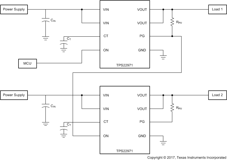
The TPS22971 has an integrated power good indicator which can be used for power sequencing. As shown in Figure 26, the switch to the second load is controlled by the PG signal from the first switch. This ensures that the power to load 2 is only enabled after the same power to load 1 is enabled after the first switch has turned on.
 Figure 26. Power Sequencing
9.2 Typical Application
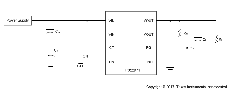
 Figure 27. Typical Application Circuit
9.2.1 Design Requirements
For this design example, below, use the input parameters shown in Table 2.
Table 2. Design Parameters
| DESIGN PARAMETER | EXAMPLE VALUE |
|---|---|
| VIN | 3.6 V |
| ILOAD | 10 mA |
| Load Capacitance (CL) | 33 μF |
| Maximum Voltage Drop | 1% |
| Maximum Inrush Current | 630 mA |
9.2.2 Detailed Design Procedure
9.2.2.1 Maximum Voltage Drop and On-Resistance
At 3.6-V input voltage, with a maximum voltage drop tolerance of 1%, the TPS22971 has a typical RON of 6.7 mΩ. The rail is supplying 10 mA of current; the voltage drop for a rail is calculated based on Equation 10.


The maximum voltage drop is 1% which is 36 mV. The voltage drop caused by the load current across the on resistance is 0.067 mV.
9.2.2.2 Managing Inrush Current
When the switch is enabled, the output capacitors must be charged up from 0 V to VIN. This charge arrives in the form of inrush current. Given a load capacitance (CL) of 33 μF, an input voltage (VIN) of 3.6V and a maximum inrush (IINRUSH) of 630 mA, use Equation 12 and Equation 13 to solve for Slew Rate (SR).


Now that the desired slew rate has been calculated, use SR and VIN in in Equation 14 to calculate a CT capacitance value.

A capacitance value of 1007pF is a non-standard value therefore a 1000 pF CT capacitance is used moving forward.
The calculated CT value can be used with Equation 2 and Equation 4 to determine tON and tPG,ON, respectively as shown in Equation 15 and Equation 16.


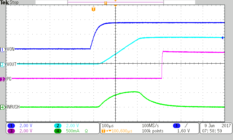
9.2.3 Application Curves

| VIN = 3.6 V | VON = 3.6 V | CIN = 1 µF |
| RL = OPEN | TA = 25°C | CL = 33 µF |

| VIN = 3.6 V | VON = 3.6 V | CIN = 1 µF |
| RL = OPEN | TA = 25°C | CL = 33 µF |