JAJSDN1B April 2017 – December 2017 TPS22971
PRODUCTION DATA.
8 Detailed Description
8.1 Overview
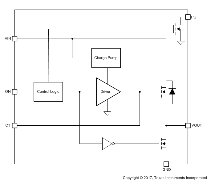
The TPS22971 is a single channel, 3-A load switch in a small, space-saving WCSP-8 package. This device implements a low resistance N-channel MOSFET with a controlled rise time for applications that need to limit the inrush current.
The controlled rise time for the device greatly reduces inrush current caused by large bulk load capacitances, thereby reducing or eliminating power supply droop. The adjustable slew rate through CT provides the design flexibility to trade off the inrush current and power up timing requirements. Integrated PG indicator notifies the system about the status of the load switch to facilitate seamless power sequencing.
This device is also designed to have very low leakage current during off state, which prevents downstream circuits from pulling high standby current from the supply. Integrated control logic, driver, power supply, and output discharge FET eliminates the need for additional external components, which reduces solution size and bill of materials (BOM) count.
8.2 Functional Block Diagram

8.3 Feature Description
8.3.1 On and Off Control
The ON pin controls the state of the switch. Asserting ON high enables the switch. ON has a low threshold, making it capable of interfacing with low-voltage signals. The ON pin is compatible with standard GPIO logic. It can be used with any microcontroller with 1.2-V, 1.8-V, 2.5-V or 3.3-V GPIOs. This pin does not have an internal bias and must not be left floating for proper functionality.
8.3.2 Controlled Turn-On
The TPS22971 has controlled Turn-On for inrush current control. A capacitor to GND on the CT pin adjusts the slew rate. For a given input voltage and desired slew rate, Equation 1 can be used to find the required CT value. For calculated CT values less than 220 pF, use 0 pF instead when solving for tON and tPG,ON.

where
- CT is the capacitor on the CT pin (in pF)
- VIN is the input voltage (in V)
- SR is the desired slew rate (in V/µs)
The CT value determined in Equation 1 can be used to find the total Turn-On time, tON, in Equation 2 or Equation 3 depending on VIN.


where
- tON is the Turn-On time (in µs)
- CT is the capacitor on the CT pin (in pF)
- VIN is the input voltage (in V)
8.3.3 Power Good (PG)
The TPS22971 has a power good (PG) output signal to indicate the gate of the pass FET is driven high and the switch is fully on (full load ready). The signal is an active high and open drain output which can be connected to a voltage source through an external pull up resistor, RPU. This voltage source can be VOUT from the TPS22971 or another external voltage. Equation 4 and Equation 5 show the approximate equation for the relationship between CT setting, VIN and PG Turn-On time (tPG,ON):


where
- tPG,ON is the PG Turn-On time (in µs)
- VIN is the input voltage (in V)
- CT is the capacitance value on the CT pin (in pF)
8.3.4 Quick Output Discharge (QOD)
The TPS22971 includes a QOD feature. When the switch is disabled, a discharge resistor is connected between VOUT and GND. This resistor has a typical value of 150 Ω and prevents the output from floating while the switch is disabled. The QOD pull-down resistance can vary with input voltage and temperature, see Figure 4.
8.4 Device Functional Modes
Table 1 lists the functional modes for the TPS22971.
Table 1. Function Table
| TPS22971 | |||
|---|---|---|---|
| ON-Pin | VIN to VOUT | VOUT to GND | PG to GND |
| Below VIL | OFF | ON | ON |
| Above VIH | ON | OFF | OFF |