JAJSE38F November 2017 – November 2023 TCAN1043-Q1 , TCAN1043G-Q1 , TCAN1043H-Q1 , TCAN1043HG-Q1
PRODUCTION DATA
- 1
- 1 特長
- 2 アプリケーション
- 3 概要
- 4 Device Comparison Table
- 5 Pin Configuration and Functions
- 6 Specifications
- 7 Parameter Measurement Information
-
8 Detailed Description
- 8.1 Overview
- 8.2 Functional Block Diagram
- 8.3 Feature Description
- 8.4 Device Functional Modes
- 9 Application Information Disclaimer
- 10Device and Documentation Support
- 11Revision History
- 12Mechanical, Packaging, and Orderable Information
8.4.6.2 Local Wake Up (LWU) via WAKE Input Terminal
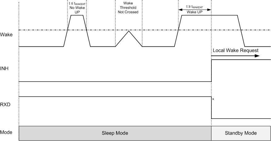
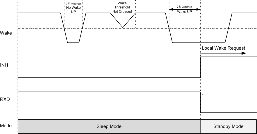
The WAKE terminal is a high voltage input terminal which can be used for local wake up (LWU) requests via a voltage transition. The terminal triggers a local wake up (LWU) event on either a low-to-high, or a high-to-low transition since it has a bi-directional input threshold (falling or rising edge).
This terminal may be used with a switch to VSUP or to ground. If the terminal is unused it should be pulled to ground or VSUP to avoid unwanted parasitic wake up events.
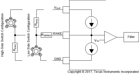
 Figure 8-6 TCAN1043xx-Q1 WAKE Circuit Example
Figure 8-6 shows two possible configurations for the WAKE terminal, the low-side and high side switch configurations. The objective of the series resistor, RSERIES, is to protect the WAKE pin of the transceiver from over current conditions that may occur in the event of a ground shift or ground loss. The minimum value of RSERIES can be calculated using the maximum supply voltage, VSUPMAX and the maximum allowable current of the WAKE pin, IIO(WAKE). RSERIES is calculated using:
If the battery voltage never exceeds 58 V DC, then the RSERIES value is approximately 20 kΩ.
The RBIAS resistor is used to set the static voltage level of the WAKE pin when the switch is not in use. When the switch is in use in a high-side switch configuration, the RBIAS resistor in combination with the RSERIES resistor sets the WAKE pin voltage appropriately above the VIH threshold. The maximum value of RBIAS can be calculated using the maximum supply voltage, VSUPMAX, the maximum WAKE threshold voltage VIH, the maximum WAKE input current IIH and the series resistor value RSERIES. RBIAS is calculated using:
If the battery voltage never exceed 58 V DC, then the RBIAS resistor value must be less than 60 kΩ.
For lower current consumption, the low-side switch configuration is the ideal architecture.
The LWU circuitry is active in Section 8.4.6, Section 8.4.4 and Section 8.4.5. If a valid LWU event occurs the device transitions to standby mode. The LWU circuitry is not active in Normal mode or Silent mode.
To minimize system level current consumption, the internal bias voltages of the terminal follows the state on the terminal with a delay of tWAKE(min). A constant high level on WAKE has an internal pull-up to VSUP and a constant low level on WAKE has an internal pull-down to GND. This minimizes the current flowing into the WAKE pin under these steady-state conditions so that it does not need to be factored into calculations of the total draw from VSUP.

