JAJSE50 November   2017 TLA2021 , TLA2022 , TLA2024

PRODUCTION DATA.  

  1. 特長
  2. アプリケーション
  3. 概要
    1.     Device Images
      1.      システム監視アプリケーションの例
  4. 改訂履歴
  5. 概要(続き)
  6. Device Comparison Table
  7. Pin Configuration and Functions
    1.     Pin Functions
  8. Specifications
    1. 8.1 Absolute Maximum Ratings
    2. 8.2 ESD Ratings
    3. 8.3 Recommended Operating Conditions
    4. 8.4 Thermal Information
    5. 8.5 Electrical Characteristics
    6. 8.6 I2C Timing Requirements
    7. 8.7 Typical Characteristics
  9. Detailed Description
    1. 9.1 Overview
    2. 9.2 Functional Block Diagrams
    3. 9.3 Feature Description
      1. 9.3.1 Multiplexer
      2. 9.3.2 Analog Inputs
      3. 9.3.3 Full-Scale Range (FSR) and LSB Size
      4. 9.3.4 Voltage Reference
      5. 9.3.5 Oscillator
      6. 9.3.6 Output Data Rate and Conversion Time
    4. 9.4 Device Functional Modes
      1. 9.4.1 Reset and Power-Up
      2. 9.4.2 Operating Modes
        1. 9.4.2.1 Single-Shot Conversion Mode
        2. 9.4.2.2 Continuous-Conversion Mode
    5. 9.5 Programming
      1. 9.5.1 I2C Interface
        1. 9.5.1.1 I2C Address Selection
        2. 9.5.1.2 I2C Interface Speed
        3. 9.5.1.3 Serial Clock (SCL) and Serial Data (SDA)
        4. 9.5.1.4 I2C Data Transfer Protocol
        5. 9.5.1.5 Timeout
        6. 9.5.1.6 I2C General-Call (Software Reset)
      2. 9.5.2 Reading and Writing Register Data
        1. 9.5.2.1 Reading Conversion Data or the Configuration Register
        2. 9.5.2.2 Writing the Configuration Register
      3. 9.5.3 Data Format
  10. 10Register Maps
    1. 10.1 Conversion Data Register (RP = 00h) [reset = 0000h]
      1. Table 6. Conversion Data Register Field Descriptions
    2. 10.2 Configuration Register (RP = 01h) [reset = 8583h]
      1. Table 7. Configuration Register Field Descriptions
  11. 11Application and Implementation
    1. 11.1 Application Information
      1. 11.1.1 Basic Interface Connections
      2. 11.1.2 Connecting Multiple Devices
      3. 11.1.3 Single-Ended Signal Measurements
      4. 11.1.4 Analog Input Filtering
      5. 11.1.5 Duty Cycling To Reduce Power Consumption
      6. 11.1.6 I2C Communication Sequence Example
    2. 11.2 Typical Application
      1. 11.2.1 Design Requirements
      2. 11.2.2 Detailed Design Procedure
      3. 11.2.3 Application Curve
  12. 12Power Supply Recommendations
    1. 12.1 Power-Supply Sequencing
    2. 12.2 Power-Supply Decoupling
  13. 13Layout
    1. 13.1 Layout Guidelines
    2. 13.2 Layout Example
  14. 14デバイスおよびドキュメントのサポート
    1. 14.1 デバイス・サポート
      1. 14.1.1 デベロッパー・ネットワークの製品に関する免責事項
    2. 14.2 関連リンク
    3. 14.3 ドキュメントの更新通知を受け取る方法
    4. 14.4 コミュニティ・リソース
    5. 14.5 商標
    6. 14.6 静電気放電に関する注意事項
    7. 14.7 Glossary
  15. 15メカニカル、パッケージ、および注文情報

Multiplexer

Figure 8 shows that the TLA2024 contains an analog input multiplexer (MUX). Four single-ended or two differential signals can be measured. Additionally, AIN0 and AIN1 can be measured differentially to AIN3. The multiplexer is configured by bits MUX[2:0] in the configuration register. When single-ended signals are measured, the negative input of the ADC is internally connected to GND by a switch within the multiplexer.
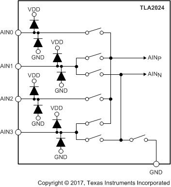
TLA2021 TLA2022 TLA2024 ai_mux_bas846.gifFigure 8. Input Multiplexer

The TLA2021 and TLA2022 do not have an input multiplexer and can either measure one differential signal or one single-ended signal. For single-ended measurements, connect the AIN1 pin to GND externally. In subsequent sections of this data sheet, AINP refers to AIN0 and AINN refers to AIN1 for the TLA2021 and TLA2022.

Electrostatic discharge (ESD) diodes connected to VDD and GND protect the TLA202x analog inputs. Keep the absolute voltage on any input within the range shown in Equation 1 to prevent the ESD diodes from turning on.

Equation 1. GND – 0.3 V < V(AINX) < VDD + 0.3 V

If the voltages on the analog input pins can potentially violate these conditions, use external Schottky diodes and series resistors to limit the input current to safe values (see the Absolute Maximum Ratings table).