JAJSEO7I October 2008 – December 2017 TPS23754 , TPS23754-1 , TPS23756
PRODUCTION DATA.
- 1 特長
- 2 アプリケーション
- 3 概要
- 4 改訂履歴
- 5 概要(続き)
- 6 Pin Configuration and Functions
- 7 Specifications
-
8 Detailed Description
- 8.1 Overview
- 8.2 Functional Block Diagram
- 8.3 Feature Description
- 8.4
Device Functional Modes
- 8.4.1
PoE Overview
- 8.4.1.1 Threshold Voltages
- 8.4.1.2 PoE Start-Up Sequence
- 8.4.1.3 Detection
- 8.4.1.4 Hardware Classification
- 8.4.1.5 Inrush and Start-Up
- 8.4.1.6 Maintain Power Signature
- 8.4.1.7 Start-Up and Converter Operation
- 8.4.1.8 PD Hotswap Operation
- 8.4.1.9 Converter Controller Features
- 8.4.1.10 Bootstrap Topology
- 8.4.1.11 Current Slope Compensation and Current Limit
- 8.4.1.12 Blanking – RBLNK
- 8.4.1.13 Dead Time
- 8.4.1.14 FRS and Synchronization
- 8.4.1.15 T2P, Start-Up, and Power Management
- 8.4.1.16 Thermal Shutdown
- 8.4.1.17 Adapter ORing
- 8.4.1.18 PPD ORing Features
- 8.4.1.19 Using DEN to Disable PoE
- 8.4.1.20 ORing Challenges
- 8.4.1
PoE Overview
-
9 Application and Implementation
- 9.1 Application Information
- 9.2
Typical Application
- 9.2.1 Design Requirements
- 9.2.2
Detailed Design Procedure
- 9.2.2.1 Input Bridges and Schottky Diodes
- 9.2.2.2 Protection, D1
- 9.2.2.3 Capacitor, C1
- 9.2.2.4 Detection Resistor, RDEN
- 9.2.2.5 Classification Resistor, RCLS
- 9.2.2.6 Dead Time Resistor, RDT
- 9.2.2.7 Switching Transformer Considerations and RVC
- 9.2.2.8 Special Switching MOSFET Considerations
- 9.2.2.9 Thermal Considerations and OTSD
- 9.2.2.10 APD Pin Divider Network, RAPD1, RAPD2
- 9.2.2.11 PPD Pin Divider Network, RPPD1, RPPD2
- 9.2.2.12 Setting Frequency (RFRS) and Synchronization
- 9.2.2.13 Current Slope Compensation
- 9.2.2.14 Blanking Period, RBLNK
- 9.2.2.15 Estimating Bias Supply Requirements and CVC
- 9.2.2.16 T2P Pin Interface
- 9.2.2.17 Advanced ORing Techniques
- 9.2.2.18 Soft Start
- 9.2.2.19 Frequency Dithering for Conducted Emissions Control
- 9.2.3 Application Curves
- 10Power Supply Recommendations
- 11Layout
- 12デバイスおよびドキュメントのサポート
- 13メカニカル、パッケージ、および注文情報
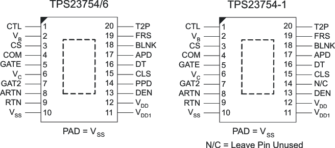
6 Pin Configuration and Functions
PWP Package
20-Pin HTSSOP
Top View

Pin Functions
| PIN | TYPE | DESCRIPTION | ||
|---|---|---|---|---|
| NAME | TPS23754
and TPS23756 |
TPS23754-1 | ||
| APD | 17 | 17 | I | Raising VAPD – VARTN above 1.5 V disables the internal hotswap switch, turns class off, and forces T2P active. This forces power to come from a external VDD1-RTN adapter. Tie APD to ARTN when not used. |
| ARTN | 8 | 8 | — | ARTN is the DC-DC converter analog return. Tie to RTN and COM on the circuit board. |
| BLNK | 18 | 18 | I | Connect to ARTN to use the internally set current-sense blanking period, or connect a resistor from BLNK to ARTN to program a more accurate period. |
| CLS | 15 | 15 | I | Connect a resistor from CLS to VSS to program classification current. 2.5 V is applied to the program resistor during classification to set class current. |
| COM | 4 | 4 | — | Gate driver return, connect to ARTN and RTN. |
| CS | 3 | 3 | I/O | DC-DC converter switching MOSFET current sense input. See RCS in Figure 27. |
| CTL | 1 | 1 | I | The control loop input to the pulse-width modulator (PWM), typically driven by output regulation feedback (for example, optocoupler). Use VB as a pullup for CTL. |
| DEN | 13 | 13 | I/O | Connect a 24.9-kΩ resistor from DEN to VDD to provide the PoE detection signature. Pulling this pin to VSS during powered operation causes the internal hotswap MOSFET to turn off. |
| DT | 16 | 16 | I | Connect a resistor from DT to ARTN to set the GATE to GAT2 dead time. Tie DT to VB to disable GAT2 operation. |
| FRS | 19 | 19 | I | Connect a resistor from FRS to ARTN to program the converter switching frequency. FRS may be used to synchronize the converter to an external timing source. |
| GATE | 5 | 5 | O | Gate drive output for the main DC-DC converter switching MOSFET. |
| GAT2 | 7 | 7 | O | Gate drive output for a second DC-DC converter switching MOSFET (see Figure 27). |
| NC | — | 14 | — | Float this no-connect pin. |
| PAD | — | — | — | Connect to VSS. |
| PPD | 14 | — | I | Raising VPPD-VSS above 1.55 V enables the hotswap MOSFET and activates T2P. Connecting PPD to VDD enables classification when APD is active. Tie PPD to VSS or float when not used. |
| RTN | 9 | 9 | — | RTN is the output of the PoE hotswap MOSFET. |
| T2P | 20 | 20 | O | Active low output that indicates a PSE has performed the IEEE 802.3at type 2 hardware classification, PPD is active, or APD is active. |
| VB | 2 | 2 | O | 5.1-V bias rail for DC-DC control circuits and the feedback optocoupler. Typically bypass with a 0.1 μF to ARTN. |
| VC | 6 | 6 | I/O | DC-DC converter bias voltage. Connect a 0.47 μF (minimum) ceramic capacitor to ARTN at the pin, and a larger capacitor to power start-up. |
| VDD | 12 | 12 | I | Connect to the positive PoE input power rail. VDD powers the PoE interface circuits. Bypass with a 0.1-μF capacitor and protect with a TVS. |
| VDD1 | 11 | 11 | I | Source of DC-DC converter start-up current. Connect to VDD for many applications. |
| VSS | 10 | 10 | — | Connect to the negative power rail derived from the PoE source. |