JAJSFC2C May   2011  – April 2018 TPS61260 , TPS61261

PRODUCTION DATA.  

  1. 特長
  2. アプリケーション
  3. 概要
    1.     Device Images
  4. 改訂履歴
  5. Pin Configuration and Functions
    1.     Pin Functions
  6. Specifications
    1. 6.1 Absolute Maximum Ratings
    2. 6.2 Handling Ratings
    3. 6.3 Recommended Operating Conditions
    4. 6.4 Thermal Information
    5. 6.5 Electrical Characteristics
    6. 6.6 Typical Characteristics
  7. Parameter Measurement Information
    1. 7.1 Schematic and List of Components
  8. Detailed Description
    1. 8.1 Overview
    2. 8.2 Functional Block Diagrams
    3. 8.3 Feature Description
      1. 8.3.1 Controller Circuit
      2. 8.3.2 Synchronous Boost Operation
      3. 8.3.3 Power Save Mode
      4. 8.3.4 Device Enable
      5. 8.3.5 Softstart and Short Circuit Protection
    4. 8.4 Device Functional Modes
      1. 8.4.1 Undervoltage Lockout
      2. 8.4.2 Output Overvoltage Protection
    5. 8.5 Programming
      1. 8.5.1 Programming the Output Voltage
      2. 8.5.2 Programming the Output Current
  9. Application and Implementation
    1. 9.1 Application Information
    2. 9.2 Typical Applications
      1. 9.2.1 TPS61260 3.3-V Output Application
        1. 9.2.1.1 Design Requirements
        2. 9.2.1.2 Detailed Design Procedure
          1. 9.2.1.2.1 Inductor Selection
          2. 9.2.1.2.2 Capacitor Selection
            1. 9.2.1.2.2.1 Input Capacitor
            2. 9.2.1.2.2.2 Output Capacitor
        3. 9.2.1.3 TPS61260 3.3-V Output Application Performance Plots
      2. 9.2.2 TPS61261 Application as LED Driver
        1. 9.2.2.1 Design Requirements
        2. 9.2.2.2 Detailed Design Procedure
        3. 9.2.2.3 TPS61261 Application as LED Driver Performance Plots
  10. 10Power Supply Recommendations
  11. 11Layout
    1. 11.1 Layout Guidelines
    2. 11.2 Layout Example
    3. 11.3 Thermal Considerations
  12. 12デバイスおよびドキュメントのサポート
    1. 12.1 デバイス・サポート
      1. 12.1.1 デベロッパー・ネットワークの製品に関する免責事項
    2. 12.2 ドキュメントのサポート
      1. 12.2.1 関連資料
    3. 12.3 関連リンク
    4. 12.4 商標
    5. 12.5 静電気放電に関する注意事項
    6. 12.6 Glossary
  13. 13メカニカル、パッケージ、および注文情報

Typical Characteristics

Table of Graphs

DESCRIPTION FIGURE
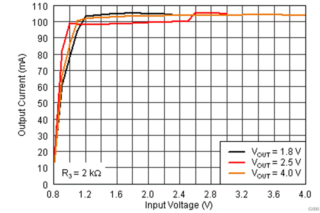
Maximum output current vs Input voltage (TPS61260, VOUT = {1.8 V; 2.5 V; 4.0 V}) Figure 1
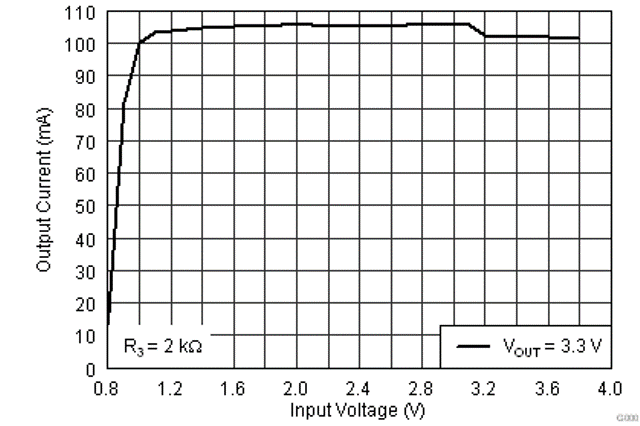
vs Input voltage (TPS61261, VOUT = 3.3 V) Figure 2
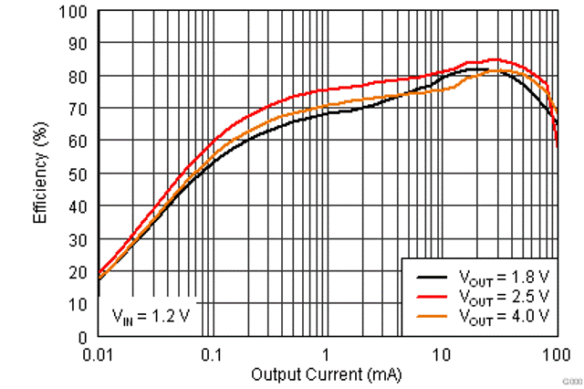
Efficiency vs Output current (TPS61260, VOUT = {1.8 V; 2.5 V; 4.0 V}) Figure 3
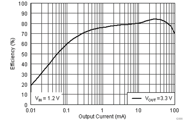
vs Output current (TPS61261, VOUT = 3.3 V) Figure 4
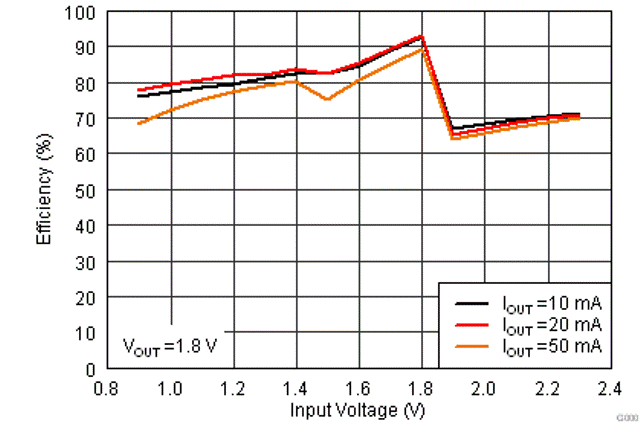
vs Input voltage (TPS61260, VOUT = 1.8 V, IOUT = {10; 20; 50 mA}) Figure 5
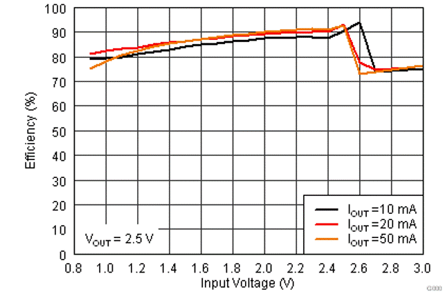
vs Input voltage (TPS61260, VOUT = 2.5 V, IOUT = {10; 20; 50 mA}) Figure 6
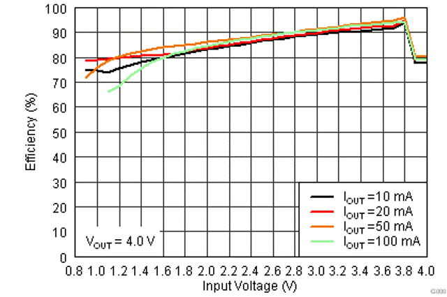
vs Input voltage (TPS61260, VOUT = 4.0 V, IOUT = {10; 20; 50; 100 mA}) Figure 7
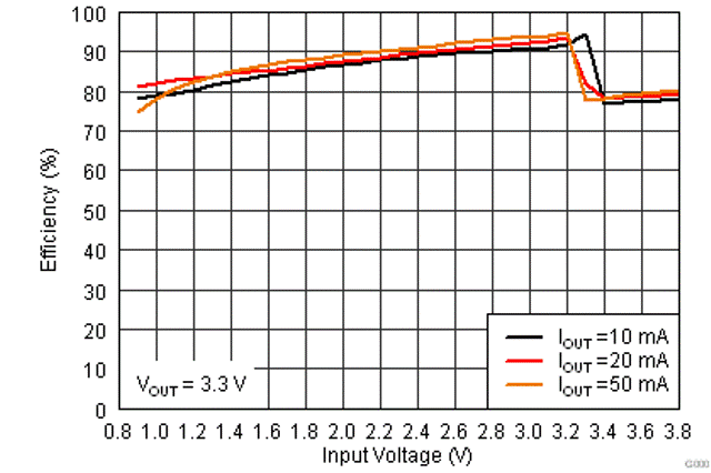
vs Input voltage (TPS61261, VOUT = 3.3V, IOUT = {10; 20; 50 mA}) Figure 8
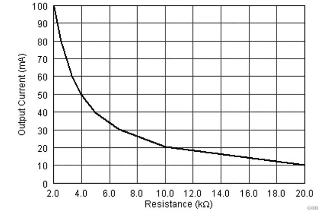
Output current vs Resistance at RI Figure 9
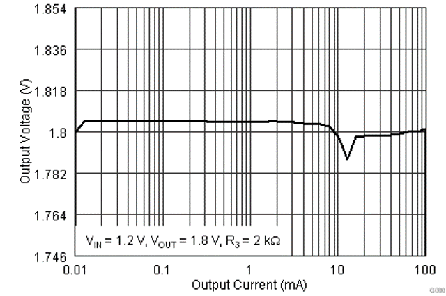
Output voltage vs Output current (TPS61260, VOUT = 1.8 V) Figure 10
vs Output current (TPS61260, VOUT = 2.5 V) Figure 11
vs Output current (TPS61260, VOUT = 4.0 V) Figure 12
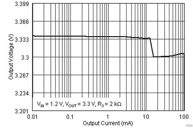
vs Output current (TPS61261, VOUT = 3.3 V) Figure 13
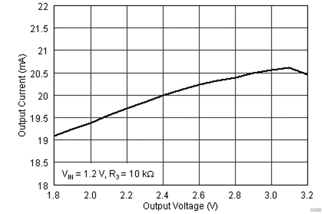
Output current vs Output voltage Figure 14
TPS61260 TPS61261 maxio1_lvsa99.gif
Figure 1. Maximum Output Current vs Input Voltage
TPS61260 TPS61261 effio1_lvsa99.gif
Figure 3. Efficiency vs Output Current
TPS61260 TPS61261 effvi1_lvsa99.gif
Figure 5. Efficiency vs Input Voltage
TPS61260 TPS61261 effvi3_lvsa99.gif
Figure 7. Efficiency vs Input Voltage
TPS61260 TPS61261 iori3_lvsa99.gifFigure 9. Output Current vs Resistance at RI
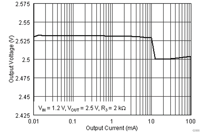
TPS61260 TPS61261 voio2_lvsa99.gif
Figure 11. Output Voltage vs Output Current
TPS61260 TPS61261 voio4_lvsa99.gif
Figure 13. Output Voltage vs Output Current
TPS61260 TPS61261 maxio2_lvsa99.gif
Figure 2. Maximum Output Current vs Input Voltage
TPS61260 TPS61261 effio2_lvsa99.gif
Figure 4. Efficiency vs Output Current
TPS61260 TPS61261 effvi2_lvsa99.gif
Figure 6. Efficiency vs Input Voltage
TPS61260 TPS61261 effvi4_lvsa99.gif
Figure 8. Efficiency vs Input Voltage
TPS61260 TPS61261 voio1_lvsa99.gifFigure 10. Output Voltage vs Output Current
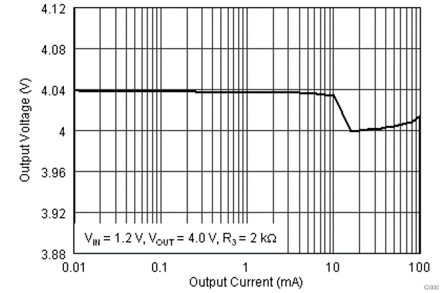
TPS61260 TPS61261 voio3_lvsa99.gif
Figure 12. Output Voltage vs Output Current
TPS61260 TPS61261 iovo1_lvsa99.gif
Figure 14. Output Current vs Output Voltage