JAJSG67F September   2018  – March 2024 TPS7H2201-SEP , TPS7H2201-SP

PRODUCTION DATA  

  1.   1
  2. 特長
  3. アプリケーション
  4. 概要
  5. Device Options
  6. Pin Configuration and Functions
  7. Specifications
    1. 6.1  Absolute Maximum Ratings
    2. 6.2  ESD Ratings
    3. 6.3  Recommended Operating Conditions
    4. 6.4  Thermal Information
    5. 6.5  Electrical Characteristics: All Devices
    6. 6.6  Electrical Characteristics: CFP and KGD Options
    7. 6.7  Electrical Characteristics: HTSSOP Option
    8. 6.8  Switching Characteristics (All Devices)
    9. 6.9  Quality Conformance Inspection
    10. 6.10 Typical Characteristics
  8. Parameter Measurement Information
  9. Detailed Description
    1. 8.1 Overview
    2. 8.2 Functional Block Diagram
    3. 8.3 Feature Description
      1. 8.3.1 Enable, Undervoltage, and Overvoltage Protection
      2. 8.3.2 Adjustable Rise Time
      3. 8.3.3 Programmable Current Limiting
      4. 8.3.4 Programmable Fault Timer
      5. 8.3.5 Current Sense
      6. 8.3.6 Parallel Operation
      7. 8.3.7 Reverse Current Protection
      8. 8.3.8 Forward Leakage Current
    4. 8.4 Device Functional Modes
  10. Application and Implementation
    1. 9.1 Application Information
    2. 9.2 Typical Applications
      1. 9.2.1 Redundancy
      2. 9.2.2 Protection
      3. 9.2.3 Design Requirements
      4. 9.2.4 Detailed Design Procedure
        1. 9.2.4.1 Undervoltage Lockout
        2. 9.2.4.2 Overvoltage Protection
        3. 9.2.4.3 Current Limit
        4. 9.2.4.4 Programmable Fault Timers
        5. 9.2.4.5 Soft Start Time
      5. 9.2.5 Application Curves
    3. 9.3 Power Supply Recommendations
    4. 9.4 Layout
      1. 9.4.1 Layout Guidelines
      2. 9.4.2 Layout Example
  11. 10Device and Documentation Support
    1. 10.1 Documentation Support
      1. 10.1.1 Related Documentation
    2. 10.2 Receiving Notification of Documentation Updates
    3. 10.3 サポート・リソース
    4. 10.4 Trademarks
    5. 10.5 静電気放電に関する注意事項
    6. 10.6 用語集
  12. 11Revision History
  13. 12Mechanical, Packaging, and Orderable Information

Typical Characteristics

GUID-470B7525-66DD-498E-845C-7DE840B56573-low.gif
IIL = 7.5 A
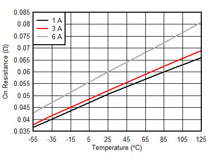
Figure 6-1 On-Resistance vs Temperature Across Loads for CFP and KGD at VIN = 1.5 V
GUID-750161C0-80FF-45D9-BCA5-52FC5FA4ACC1-low.gif
IIL = 7.5 A
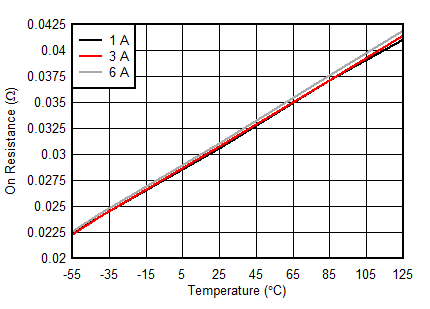
Figure 6-3 On-Resistance vs Temperature Across Loads for CFP and KGD at VIN = 7 V
GUID-20230627-SS0I-Q4VS-6PDX-XHZJ78DJL8TW-low.svg
IIL = 7.5 A
Figure 6-5 On-Resistance vs Temperature Across Loads for HTSSOP at VIN = 5 V
GUID-70DD842F-BED9-4452-8BE5-7EE90D1D4E25-low.gif
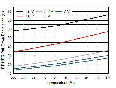
Figure 6-7 RTIMER Pull-Down Resistance vs Temperature Across VIN
GUID-1DD30DD9-0C1B-45C2-B354-E91C7BFC7359-low.gif
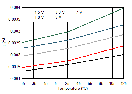
Figure 6-9 IQ vs Temperature Across VIN
GUID-EACA48CA-2D2C-4785-BE24-29BA9622373E-low.gif
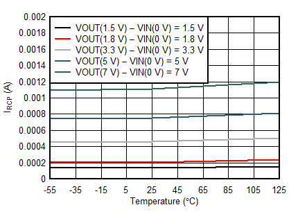
Figure 6-11 IRCP vs Temperature With EN = GND
GUID-2D67AF7C-F37B-4962-B8B4-4E6A8966C8F6-low.gif
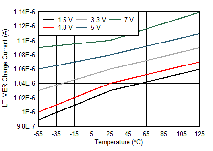
Figure 6-13 ILTIMER Charge Current vs Temperature Across VIN
GUID-BCD132F7-14FD-4175-BEEC-B9775495DDB2-low.gif
 
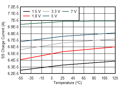
Figure 6-15 SS Charge Current vs Temperature Across VIN
GUID-3F4BFFAF-6DE3-4779-8BF1-AC82422BCD85-low.gif
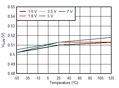
EN pin driven directly
 
Figure 6-17 VILEN vs Temperature Across VIN
GUID-1755BB31-A1BB-4036-B9D7-2D1D606ABC48-low.gif
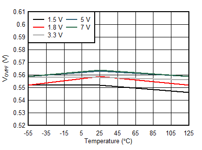
OVP pin driven directly
Figure 6-19 VOVPF vs Temperature Across VIN
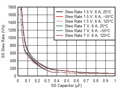
GUID-F4AFE863-E8F3-4A2F-8783-4B4D1582FFC3-low.gif
Figure 6-21 SS Slew Rate vs SS Capacitor Across Temperature
GUID-AE4881DA-54FA-46AE-A830-0036D3733249-low.gif
IIL = 7.5 A
Figure 6-2 On-Resistance vs Temperature Across Loads for CFP and KGD at VIN = 5 V
GUID-20230627-SS0I-VXPF-36VT-GKXZGJNHNWXM-low.svg
IIL = 7.5 A
Figure 6-4 On-Resistance vs Temperature Across Loads for HTSSOP at VIN = 1.5 V
GUID-20230627-SS0I-RT9K-0VG2-QCC0CZLL4Z1Z-low.svg
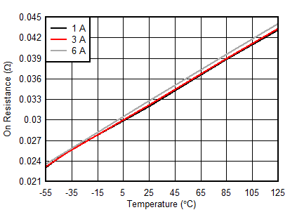
IIL = 7.5 A
Figure 6-6 On-Resistance vs Temperature Across Loads for HTSSOP at VIN = 7 V
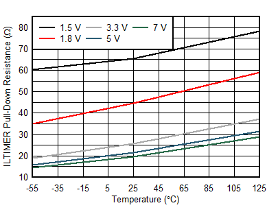
GUID-B50379CC-F437-4D18-BB50-90663AE03036-low.gif
Figure 6-8 ILTIMER Pull-Down Resistance vs Temperature Across VIN
GUID-C933BF4A-5750-416F-87DC-DDEEDD765646-low.gif
Figure 6-10 IRCP vs Temperature With EN = 7 V
GUID-E3021A91-7F7B-4AA6-A227-5D9E86E1DA0F-low.gif
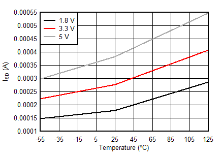
Figure 6-12 ISD VIN vs Temperature Across VIN
GUID-0A30137C-F2E5-4DAC-8507-93FC3731E774-low.gif
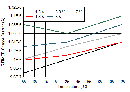
Figure 6-14 RTIMER Charge Current vs Temperature Across VIN
GUID-1BCBEFAA-27C6-478E-9094-C2A0BE3C1441-low.gif
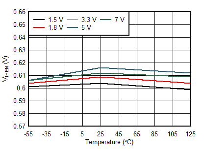
EN pin driven directly
Figure 6-16 VIHEN vs Temperature Across VIN
GUID-84856C25-A26A-42D5-A58A-7AB23455710E-low.gif
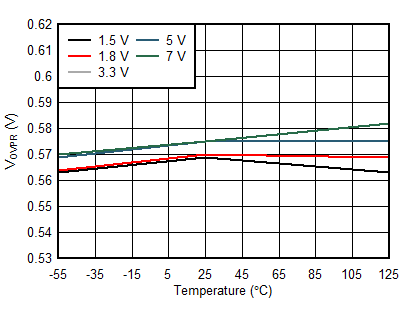
OVP pin driven directly
Waveform at 3.3 V is obscured by the 5 V
Figure 6-18 VOVPR vs Temperature Across VIN
GUID-20230127-SS0I-1B8W-542H-5ZBQ3HCPGTBG-low.svg
 
Figure 6-20 IIL vs RIL Across Temperature