JAJSKF6C November 2020 – December 2021 TPS2661
PRODUCTION DATA
- 1 特長
- 2 アプリケーション
- 3 概要
- 4 Revision History
- 5 Device Comparison Table
- 6 Pin Configuration and Functions
- 7 Specifications
-
8 Detailed Description
- 8.1 Overview
- 8.2 Functional Block Diagram
- 8.3
Feature Description
- 8.3.1 Overload Protection and Fast-Trip
- 8.3.2 Reverse Current Blocking for Unipolar Current Inputs TPS26610, TPS26611 and TPS26612 (4–20 mA, 0–20 mA)
- 8.3.3 OUTPUT and INPUT Cutoff During Overvoltage, Undervoltage Due to Miswiring
- 8.3.4 External Power Supply (±Vs)
- 8.3.5 Loop Testing Without ±Vs Supply (Loop Power Mode in TPS26610, TPS26613 Only)
- 8.3.6 Enable Control With TPS26611, TPS26612, and TPS26614
- 8.3.7 Signal Good Indicator (SGOOD)
- 8.4 Device Functional Modes
-
9 Application and Implementation
- 9.1 Application Information
- 9.2 Typical Application: Analog Input Protection for Current Inputs with TPS26610
- 9.3 Typical Application: Analog Input Protection for Multiplexed Current and Voltage Inputs with TPS26611
- 9.4 System Examples
- 10Power Supply Recommendations
- 11Layout
- 12Device and Documentation Support
- 13Mechanical, Packaging, and Orderable Information
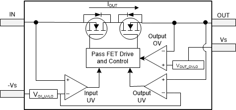
8.3.3.2 Output or Input Undervoltage With TPS26610, TPS26611 and TPS26612
TPS26610, TPS26611 and TPS26612 devices
provide protection from undervoltage events on IN and OUT pins by turning off the
internal pass FETs and cutting off the signal path whenever VOUT or
VIN goes below VO/I_UVLO threshold. The signal path through
the device is restored again when VOUT or VIN goes above
[VO/I_UVLO – VO/I_UVLO_Hyst] value. The device turns off the
internal FETs within a time of tO/I_UV_CUT after output or input voltage has
gone below VO/I_UVLO threshold. The device recovers from output or input
undervoltage within a time of tOUT_CUT_Rec after output or input voltage has
gone above [VO/I_UVLO – VO/I_UVLO_Hyst] voltage. See the Timing Requirements in Specifications for tO/I_UV_CUT and
tOUT_CUT_Rec.
 Figure 8-12 Output and Input Undervoltage
Cutoff With TPS26610, TPS26611 and TPS26612In case of overvoltage, undervoltage and miswiring events on IN and OUT pins,
voltages exceeding Absolute Maximum Ratings (see Specifications)
for IN and OUT Pins can damage the device. Figure 8-13 and Figure 8-14 illustrate the output and input undervoltage protection in these devices.
  Figure 8-13 Output Undervoltage
Protection
 Figure 8-14 Input Undervoltage
Protection
 Figure 8-12 Output and Input Undervoltage
Cutoff With TPS26610, TPS26611 and TPS26612
 Figure 8-13 Output Undervoltage
Protection
 Figure 8-14 Input Undervoltage
Protection