JAJSKR5D October 2020 – July 2024 TMUX7211 , TMUX7212 , TMUX7213
PRODUCTION DATA
- 1
- 1 特長
- 2 アプリケーション
- 3 概要
- 4 Device Comparison Table
- 5 Pin Configuration and Functions
-
6 Specifications
- 6.1 Absolute Maximum Ratings
- 6.2 ESD Ratings
- 6.3 Thermal Information
- 6.4 Recommended Operating Conditions
- 6.5 Source or Drain Continuous Current
- 6.6 ±15 V Dual Supply: Electrical Characteristics
- 6.7 ±15 V Dual Supply: Switching Characteristics
- 6.8 ±20 V Dual Supply: Electrical Characteristics
- 6.9 ±20 V Dual Supply: Switching Characteristics
- 6.10 44 V Single Supply: Electrical Characteristics
- 6.11 44 V Single Supply: Switching Characteristics
- 6.12 12 V Single Supply: Electrical Characteristics
- 6.13 12 V Single Supply: Switching Characteristics
- 6.14 Typical Characteristics
- 7 Parameter Measurement Information
- 8 Detailed Description
- 9 Application and Implementation
- 10Device and Documentation Support
- 11Revision History
- 12Mechanical, Packaging, and Orderable Information
9.2 Typical Application
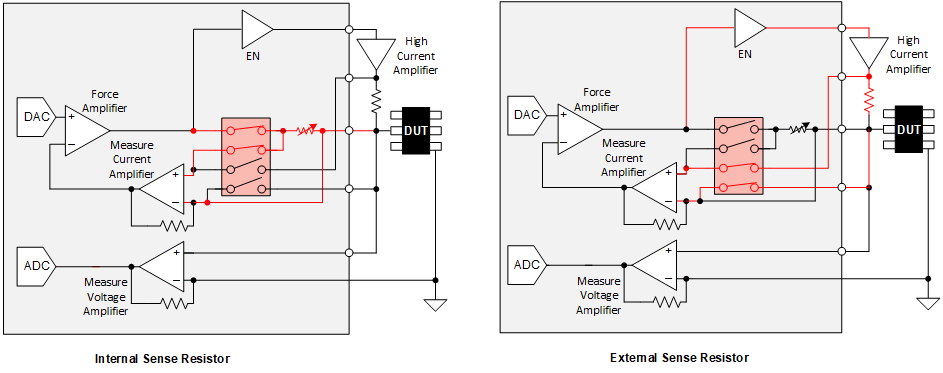
One example to take advantage of TMUX721x precision performance is the implementation of parametric measurement unit (PMU) in the semiconductor automatic test equipment (ATE) application.
In Automated Test Equipment (ATE) systems, the Parametric Measurement Unit (PMU) is tasked to measure device (DUT) parametric information in terms of voltage and current. When measuring voltage, current is applied at the DUT pin, and current range adjustment can be done through changing the value of the internal sense resistor. There is sometimes a need, depending on the DUT, to use even higher testing current than natively supported by the system. A 4 channel SPST switch, together with external higher current amplifier and resistor, can be used to achieve the flexibility. The PMU operating voltage is typically in mid voltage (up to 20 V). An appropriate switch like the TMUX721x with low leakage current (0.05 nA typical) works well in these applications to ensure measurement accuracy and low RON and flat RON_FLATNESS allows the current range to be controlled more precisely. Figure 9-1 shows simplified diagram of such implementations in memory and semiconductor test equipment.
 Figure 9-1 High
Current Range Selection Using External Resistor