JAJSKR5D October   2020  – July 2024 TMUX7211 , TMUX7212 , TMUX7213

PRODUCTION DATA  

  1.   1
  2. 特長
  3. アプリケーション
  4. 概要
  5. Device Comparison Table
  6. Pin Configuration and Functions
  7. Specifications
    1. 6.1  Absolute Maximum Ratings
    2. 6.2  ESD Ratings
    3. 6.3  Thermal Information
    4. 6.4  Recommended Operating Conditions
    5. 6.5  Source or Drain Continuous Current
    6. 6.6  ±15 V Dual Supply: Electrical Characteristics 
    7. 6.7  ±15 V Dual Supply: Switching Characteristics 
    8. 6.8  ±20 V Dual Supply: Electrical Characteristics
    9. 6.9  ±20 V Dual Supply: Switching Characteristics
    10. 6.10 44 V Single Supply: Electrical Characteristics 
    11. 6.11 44 V Single Supply: Switching Characteristics 
    12. 6.12 12 V Single Supply: Electrical Characteristics 
    13. 6.13 12 V Single Supply: Switching Characteristics 
    14. 6.14 Typical Characteristics
  8. Parameter Measurement Information
    1. 7.1  On-Resistance
    2. 7.2  Off-Leakage Current
    3. 7.3  On-Leakage Current
    4. 7.4  tON and tOFF Time
    5. 7.5  tON (VDD) Time
    6. 7.6  Propagation Delay
    7. 7.7  Charge Injection
    8. 7.8  Off Isolation
    9. 7.9  Channel-to-Channel Crosstalk
    10. 7.10 Bandwidth
    11. 7.11 THD + Noise
    12. 7.12 Power Supply Rejection Ratio (PSRR)
  9. Detailed Description
    1. 8.1 Overview
    2. 8.2 Functional Block Diagram
    3. 8.3 Feature Description
      1. 8.3.1 Bidirectional Operation
      2. 8.3.2 Rail-to-Rail Operation
      3. 8.3.3 1.8V Logic Compatible Inputs
      4. 8.3.4 Integrated Pull-Down Resistor on Logic Pins
      5. 8.3.5 Fail-Safe Logic
      6. 8.3.6 Latch-Up Immune
      7. 8.3.7 Ultra-Low Charge Injection
    4. 8.4 Device Functional Modes
    5. 8.5 Truth Tables
  10. Application and Implementation
    1. 9.1 Application Information
    2. 9.2 Typical Application
      1. 9.2.1 Design Requirements
      2. 9.2.2 Detailed Design Procedure
      3. 9.2.3 Application Curve
    3. 9.3 Power Supply Recommendations
    4. 9.4 Layout
      1. 9.4.1 Layout Guidelines
      2. 9.4.2 Layout Example
  11. 10Device and Documentation Support
    1. 10.1 Documentation Support
      1. 10.1.1 Related Documentation
    2. 10.2 ドキュメントの更新通知を受け取る方法
    3. 10.3 サポート・リソース
    4. 10.4 Trademarks
    5. 10.5 静電気放電に関する注意事項
    6. 10.6 用語集
  12. 11Revision History
  13. 12Mechanical, Packaging, and Orderable Information

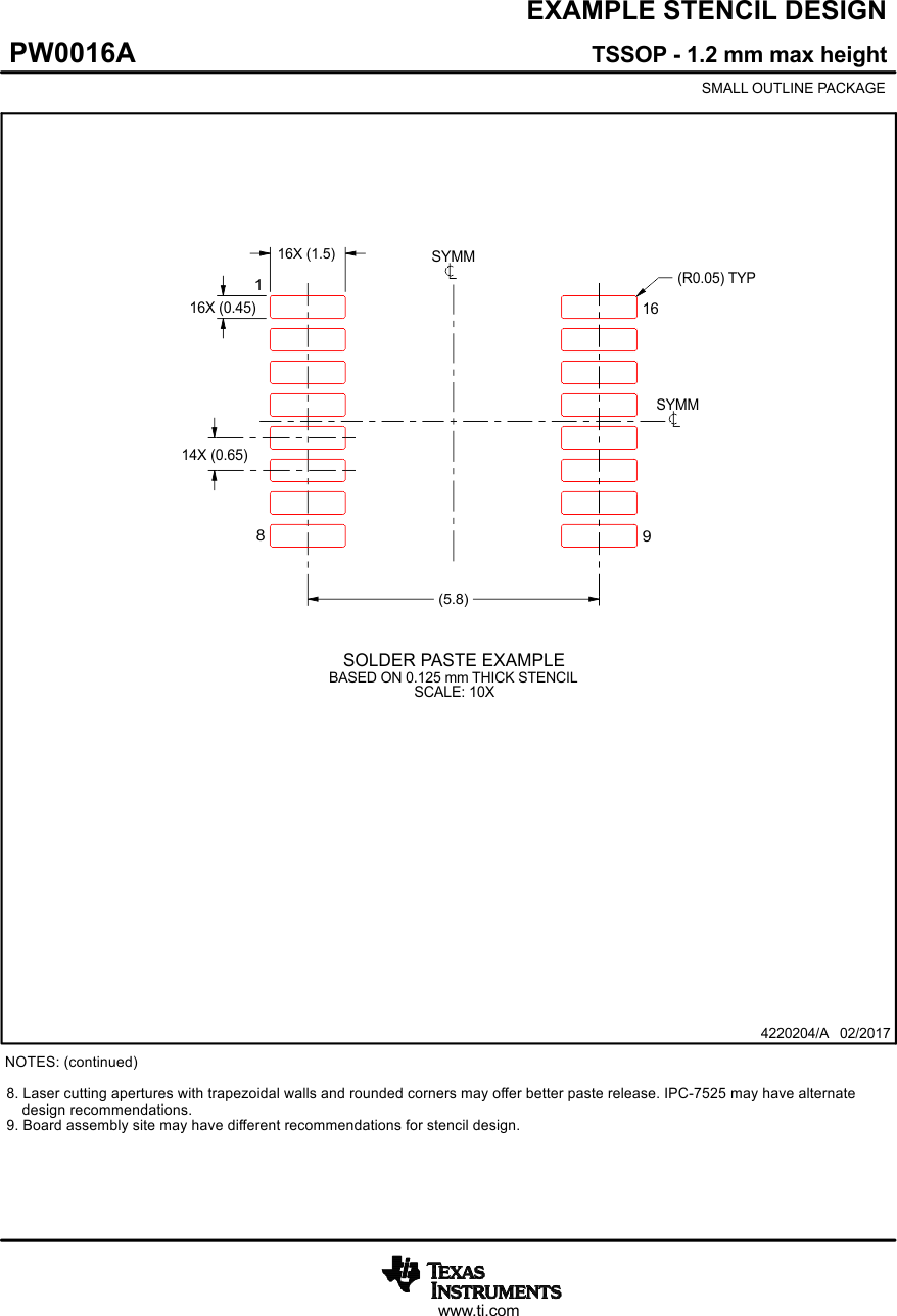
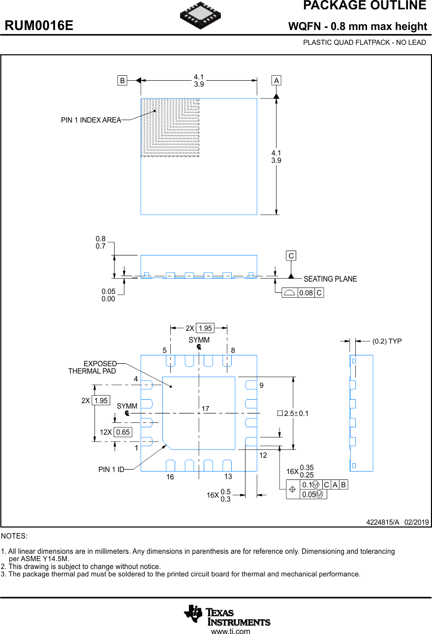
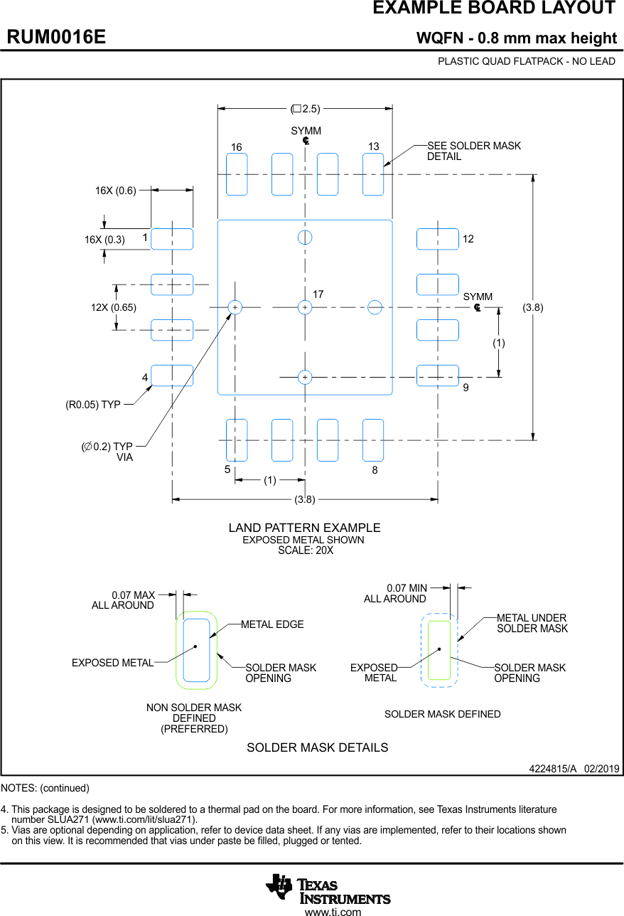
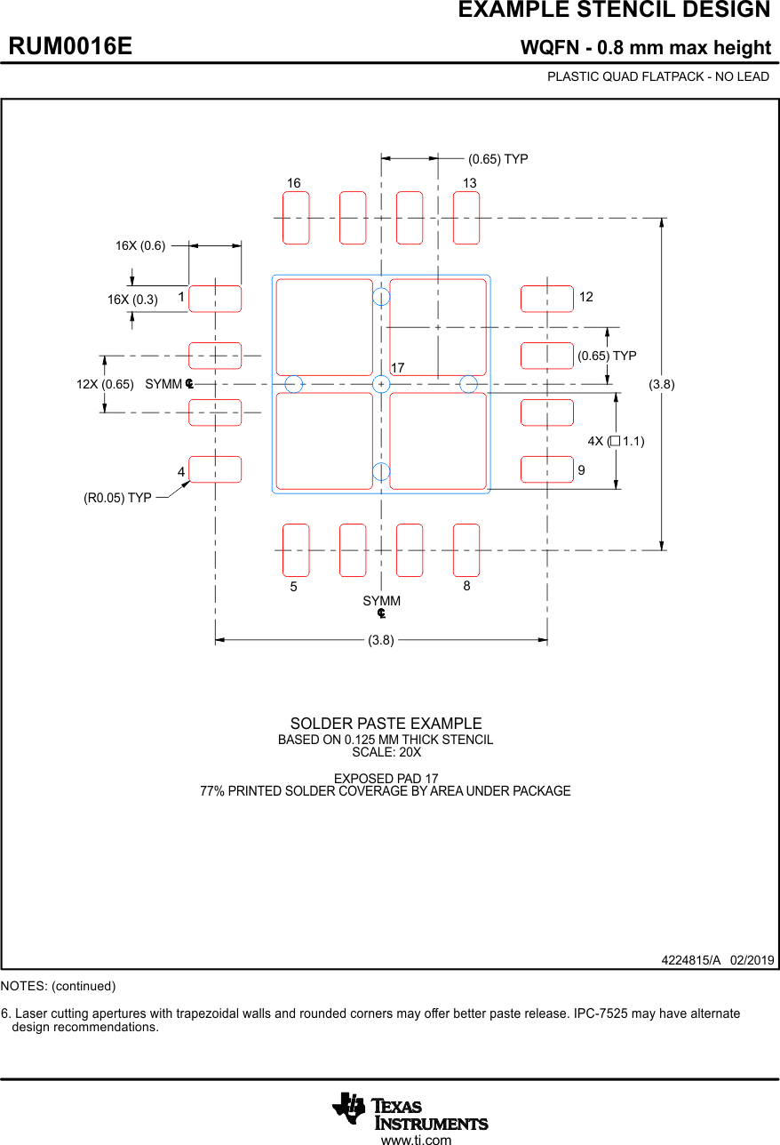
Mechanical, Packaging, and Orderable Information

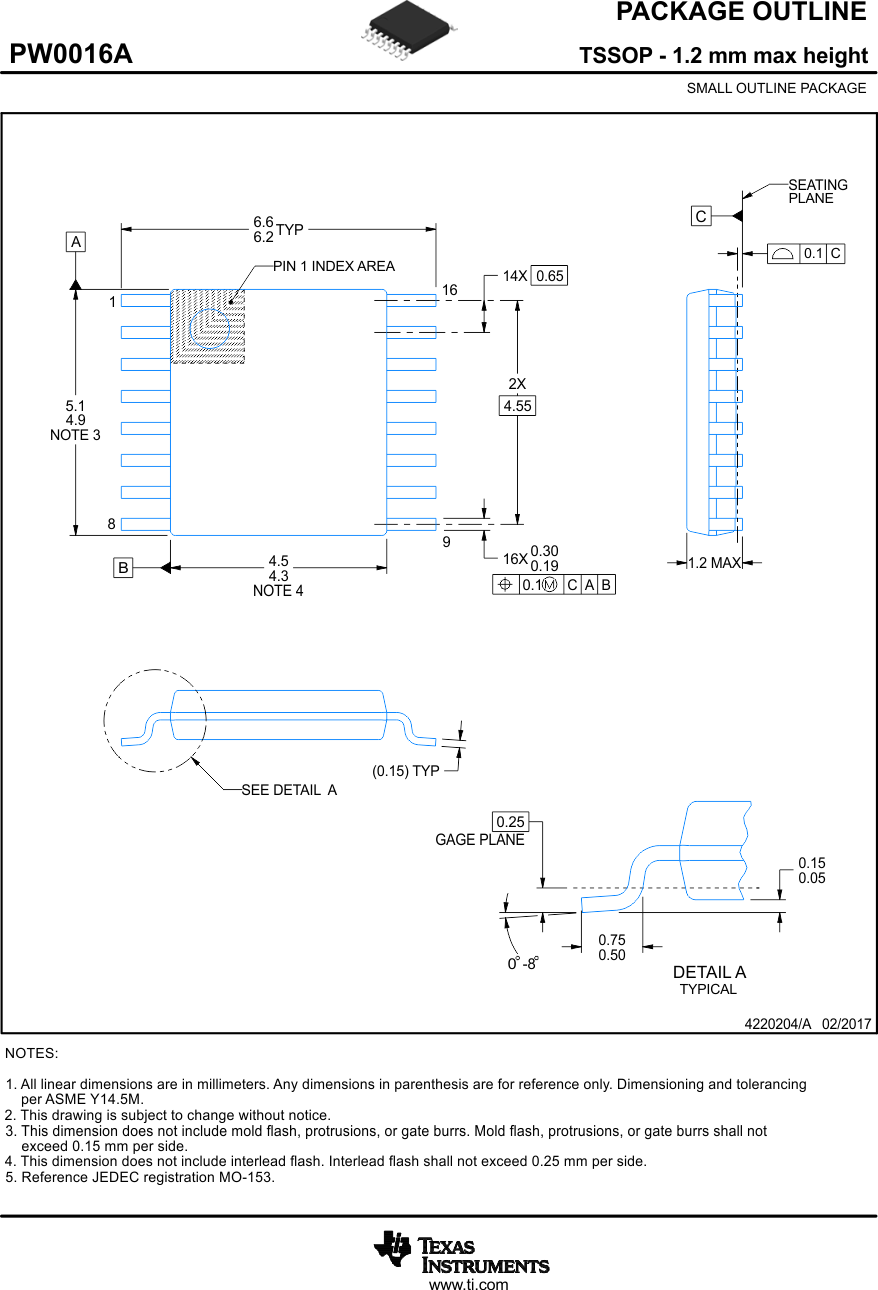
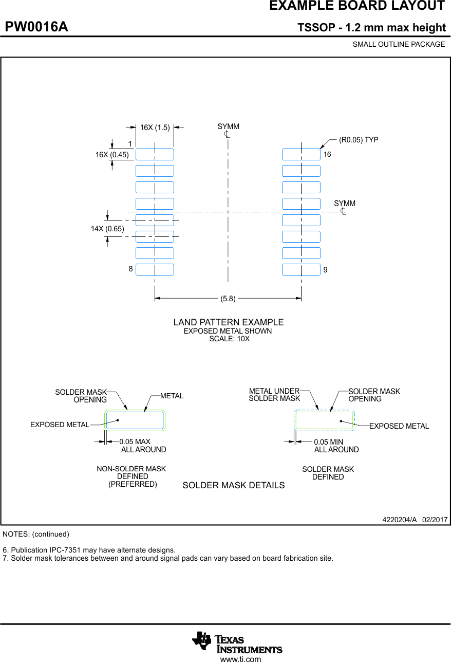
The following pages include mechanical, packaging, and orderable information. This information is the most current data available for the designated devices. This data is subject to change without notice and revision of this document. For browser-based versions of this data sheet, refer to the left-hand navigation.
TMUX7211 TMUX7212 TMUX7213