JAJSO83B May   2024  – October 2024 THVD2410V-EP , THVD2450V-EP , THVD2452V-EP

PRODUCTION DATA  

  1.   1
  2. 特長
  3. アプリケーション
  4. 概要
  5. Pin Configuration and Functions
  6. Specifications
    1. 5.1  Absolute Maximum Ratings
    2. 5.2  ESD Ratings
    3. 5.3  ESD Ratings [IEC]
    4. 5.4  Recommended Operating Conditions
    5. 5.5  Thermal Information
    6. 5.6  Power Dissipation
    7. 5.7  Electrical Characteristics
    8. 5.8  Switching Characteristics - 250 kbps
    9. 5.9  Switching Characteristics - 1 Mbps
    10. 5.10 Switching Characteristics - 20 Mbps
    11. 5.11 Switching Characteristics - 50 Mbps
    12. 5.12 Typical Characteristics
  7. Parameter Measurement Information
  8. Detailed Description
    1. 7.1 Overview
    2. 7.2 Functional Block Diagrams
    3. 7.3 Feature Description
      1. 7.3.1 ±70-V Fault Protection
      2. 7.3.2 Integrated IEC ESD and EFT Protection
      3. 7.3.3 Driver Overvoltage and Overcurrent Protection
      4. 7.3.4 Enhanced Receiver Noise Immunity
      5. 7.3.5 Receiver Fail-Safe Operation
      6. 7.3.6 Low-Power Shutdown Mode
    4. 7.4 Device Functional Modes
  9. Application and Implementation
    1. 8.1 Application Information
    2. 8.2 Typical Application
      1. 8.2.1 Design Requirements
        1. 8.2.1.1 Data Rate and Bus Length
        2. 8.2.1.2 Stub Length
        3. 8.2.1.3 Bus Loading
        4. 8.2.1.4 Transient Protection
      2. 8.2.2 Detailed Design Procedure
      3. 8.2.3 Application Curves
    3. 8.3 Power Supply Recommendations
    4. 8.4 Layout
      1. 8.4.1 Layout Guidelines
      2. 8.4.2 Layout Example
  10. Device and Documentation Support
    1. 9.1 Device Support
      1. 9.1.1 サード・パーティ製品に関する免責事項
    2. 9.2 ドキュメントの更新通知を受け取る方法
    3. 9.3 サポート・リソース
    4. 9.4 Trademarks
    5. 9.5 静電気放電に関する注意事項
    6. 9.6 用語集
  11. 10Revision History
  12. 11Mechanical, Packaging, and Orderable Information

Application Curves

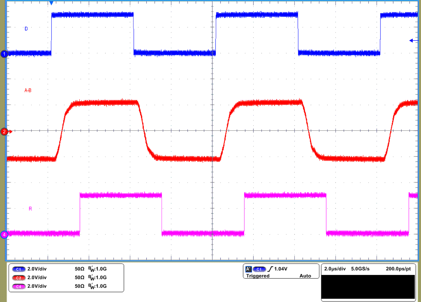
THVD2410V-EP THVD2450V-EP THVD2452V-EP THVD2410V-EP Waveforms at VCC = 3.3V
THVD2410V-EP VCC = 3.3V RL = 50Ω
Random (PRBS7) data at 250kbps
Figure 8-7 THVD2410V-EP Waveforms at VCC = 3.3V
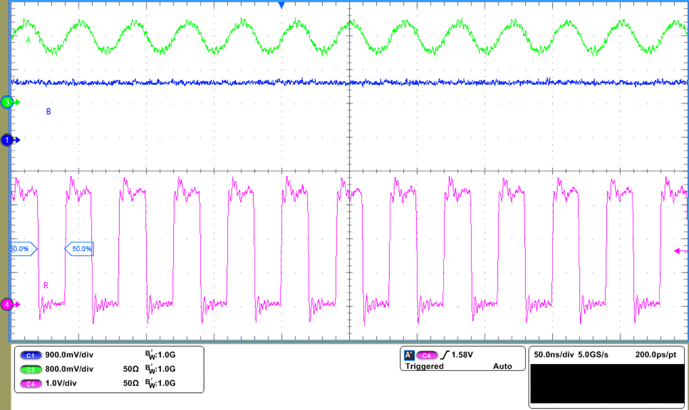
THVD2410V-EP THVD2450V-EP THVD2452V-EP THVD2450V-EP Receiver Waveforms with ±200mV
                            VID
THVD2450V-EP Pin A is supplied with ±200mV with 1.5V DC bias Pin B = 1.5V
Figure 8-9 THVD2450V-EP Receiver Waveforms with ±200mV VID
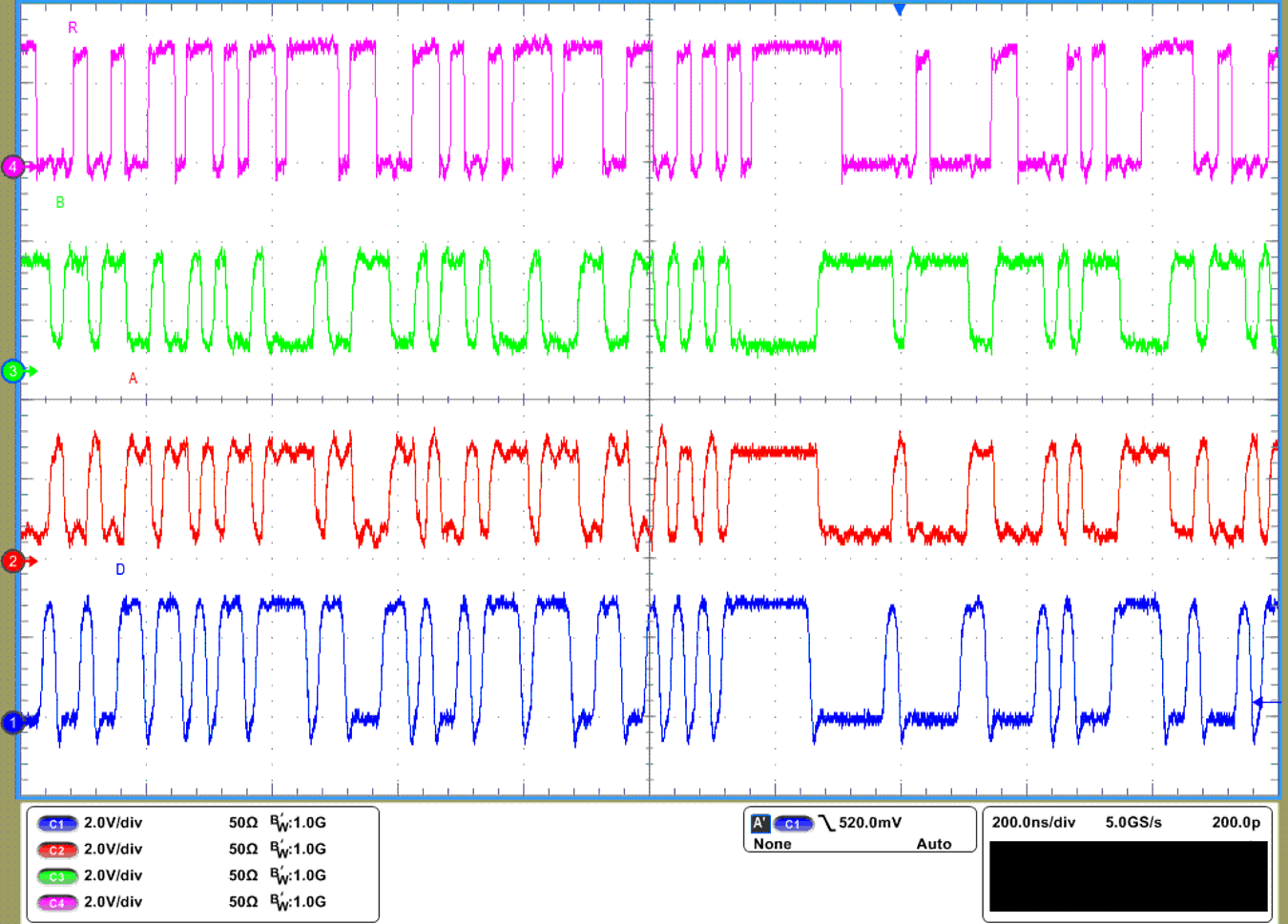
THVD2410V-EP THVD2450V-EP THVD2452V-EP THVD2450V-EP Waveforms at VCC = 3.3V
THVD2450V-EP VCC = 3.3V RL = 50Ω
Random (PRBS7) data at 50Mbps
Figure 8-8 THVD2450V-EP Waveforms at VCC = 3.3V