JAJSUN0D November 1998 – May 2024 CD4016B , CD4016B-MIL
PRODUCTION DATA
5 Parameter Measurement Information
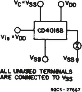 Figure 5-1 Off-state Switch Input or
Output Leakage Current Test Circuit.
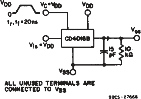 Figure 5-2 Test Circuit for
Square-wave Response.
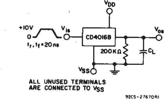 Figure 5-3 Propagation Delay Time
Signal Input (vIS) To Signal Output (vOS)
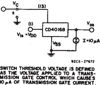 Figure 5-5 Switch Threshold
Voltage.
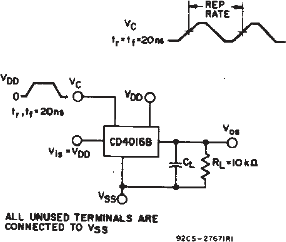 Figure 5-4 MAX Control-input
Repetition Rate.
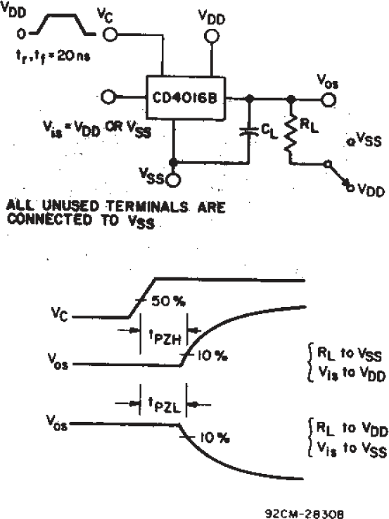 Figure 5-6 Turn-On Propagation
Delay-control Input.