SBAA345A January 2019 – September 2024 DAC80501 , DAC8551 , DAC8811 , DAC8831 , OPA227 , OPA541 , THS4011
| Power Supply | DAC Output | Voltage Output | Current Output |
|---|---|---|---|
| VCC: 24V, VSS: –5V, VDD: 5V | 0V to 2.5V | 0V to 5V | 0A to 10A |
Design Description
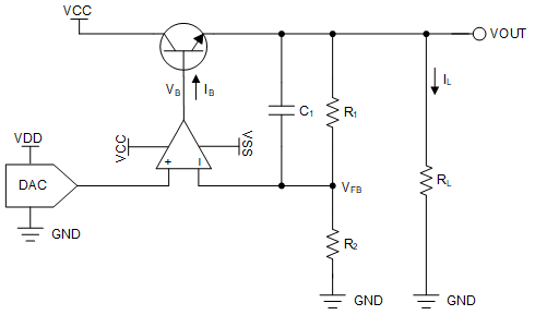
High-current voltage output can be obtained from a digital-to-analog converter (DAC) using a power amplifier at the DAC output. To have additional flexibility with amplifier performance like accuracy, bandwidth, and higher current, the circuit as shown in the following figure is an excellent choice. For example, power amplifiers typically have much higher output offset error compared to a precision amplifier. The DAC programs the output voltage along with the gain of the amplifier. The amplifier maintains the output voltage using negative feedback. The high current to the load is provided by the transistor. This circuit is useful in applications where components must be tested with different AC or DC voltage excitation such as memory and semiconductor test equipment, LCD test equipment, and others.
Design Notes
- Choose a DAC with the required resolution and output range.
- Choose an op amp with low offset and low drift to minimize error. Choose a part with sufficient gain-bandwidth product (GBW), as required by the output signal.
- Choose R1 and R2 such that the desired output voltage is met along with the DAC output voltage, along with tolerance which maintains the desired accuracy.
- Choose the compensation capacitor C1 such that it is larger than the input capacitance of the op-amp inputs.
- Choose a transistor that can provide the required load current and has a high hFE so that the base current is sufficiently smaller than the output current limit of the op amp. A bipolar-junction transistor (BJT) Darlington pair or a high-power metal-oxide semiconductor field-effect transistor (MOSFET) are preferable.
Design Steps
- The DAC80501 device is a 16-bit, single-channel, high-performance precision DAC. The DAC80501 device is specified monotonic, by design, and offers excellent linearity of less than 1LSB. These devices include a 2.5V, 5ppm/°C internal reference, giving full-scale output voltage ranges of 1.25V, 2.5V, or 5V.
- The OPA227 operational amplifier combines low noise and wide bandwidth with high precision to make it the best choice for applications requiring both AC and precision DC performance. The OPA227 device is unity-gain stable and features high slew rate (2.3V/µs) and wide bandwidth (8MHz).
- The transfer function of the output voltage is given by:

To get an output voltage of 5V with a DAC output of 2.5V, for example, chose both R1 and R2 as 10kΩ. This keeps the quiescent current through the feedback network as 5V / 20kΩ = 250µA. This current works for this design because this design is for a high-output current. In case the output current is lower, the resistance values can be increased so that the quiescent current is negligible, compared to the output current.
- The base current, IB, for the transistor for a given
load current IL is given by:
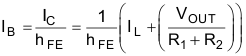
To get a maximum load current of 10A, the collector current (IC) of the transistor is approximately 10A (ignoring 250-µA quiescent current). To keep IB less than 20mA, keep hFE greater than (10A / 20mA) = 500
- In general, compensation capacitor C1 is not set by fixed equations, but rather by choosing values while observing the output small-signal step response. Through simulation in this example, select C1 ≥ 22pF.
 Figure 1-1 DC Transfer Characteristics
 Figure 1-2 Small Signal Step Response Without Compensation
 Figure 1-3 Small Signal Step Response With C1 = 22pF
Alternative Design With Power Amplifier
The following figure depicts the simplified circuit diagram of an alternative design using a power amplifier. To achieve a high-current output from the DAC, use a power amplifier like the OPA541 device. However, as previously mentioned, this circuit can have accuracy and bandwidth limitations. Depending on the system requirements, either of the circuit topologies can be used for generating high-current output. The output transfer function of this circuit is the same as the following figure.

Design Featured Devices and Alternative Parts
| Device | Key Features | Link |
|---|---|---|
| DAC80501 | 16-bit, 1-LSB INL, digital-to-analog converter (DAC) with precision internal reference | True 16-bit, 1-ch, SPI/I2C, voltage-output DAC in WSON package with precision internal reference |
| DAC8551 | 16-Bit, ultra-low glitch, voltage output, digital-to-analog converter | 16-Bit, Ultra-low Glitch, Voltage Output, Digital to Analog Converter |
| DAC8811 | 16-bit, single-channel, serial input multiplying DAC with 0.5-µs settling time | 16-bit, single-channel, serial input multiplying DAC with 0.5us settling time |
| DAC8831 | 16-bit, ultra-low power, voltage output digital-to-analog converter | 16-Bit, Ultra-Low Power, Voltage Output Digital to Analog Converter |
| OPA227 | High Precision, Low Noise Operational Amplifiers | High Precision, Low Noise Operational Amplifiers |
| OPA541 | High Power Monolithic Operational Amplifier | High Power Monolithic Operational Amplifier |
| THS4011 | 290-MHz low-distortion voltage-feedback amplifier | 290-MHz Low-Distortion Voltage-Feedback Amplifier |
Link to Key Files
Texas Instruments, SBAM417 sources files, software support