SBAA583 july 2023 PCM1820 , PCM1820-Q1 , PCM1821 , PCM1821-Q1 , PCM1822 , PCM1822-Q1 , PCM3120-Q1 , PCM5120-Q1 , PCM6120-Q1 , TLV320ADC3120 , TLV320ADC5120 , TLV320ADC6120
- 1
- Abstract
- Trademarks
- 1Introduction
- 2AC Coupling Schemes
- 3DC Coupled Scheme
-
4Application Examples
- 4.1 Electret Condenser Microphone: Single Ended DC- Coupled Input
- 4.2 Electret Condenser Microphone: Single Ended AC Coupled Input
- 4.3 Selection of a Microphone
- 4.4 Condenser Microphone: Differential DC-Coupled Input
- 4.5 Condenser Microphone: Differential AC-Coupled Input
- 4.6 MEMS Microphone: Differential AC Coupled Input
- 4.7 Circuit With No Offset and Response Down to DC
- 4.8 Improving SNR by Summing the Output of 2 ADC Channels
- 4.9 Measure a High Voltage Waveform (+-50 V)
- 4.10 I2C Listing
- 5Summary
- 6References
3.1 Biasing the Pins
Case 1: When INxP and INxM have the same static DC voltage.
. There is no DC offset in the digitized data; however, if the DC levels on the pins are close to VAVDD or VGND, there is reduced headroom for AC signals. The optimum bias level for the two pins is VREF/2. At this level, a differential range of 2 VRMS is supported.
 Figure 3-2 Optimum Biasing 1.375
VDC on INxP and INxM Pins
Figure 3-2 Optimum Biasing 1.375
VDC on INxP and INxM PinsAs shown in Figure 3-2, a 1-Vrms signal is added on a DC voltage of 1.375 V. The waveforms at INxP and INxM are 180° out-of-phase. At no point does the waveform exceed 3.3 V or go below 0 V. Thus, the analog signal of 2-Vrms differential corresponding to full scale digital data can be given to the ADC pin without distortion.
 Figure 3-3 Biasing INxP and INxM at a
Higher Voltage
Figure 3-3 Biasing INxP and INxM at a
Higher VoltageFigure 3-3 shows the pins bias at 2.8 VDC.
A larger AC signal results in the pin waveform exceeding 3.3 V and clipping. This process results in harmonic distortion; therefore, the signal handling is reduced to 1 Vp differential.
The Figure 3-4 shows a 500-mV (peak) signal with a DC offset of 2.5 V. A larger signal results in harmonics appearing on the FFT.
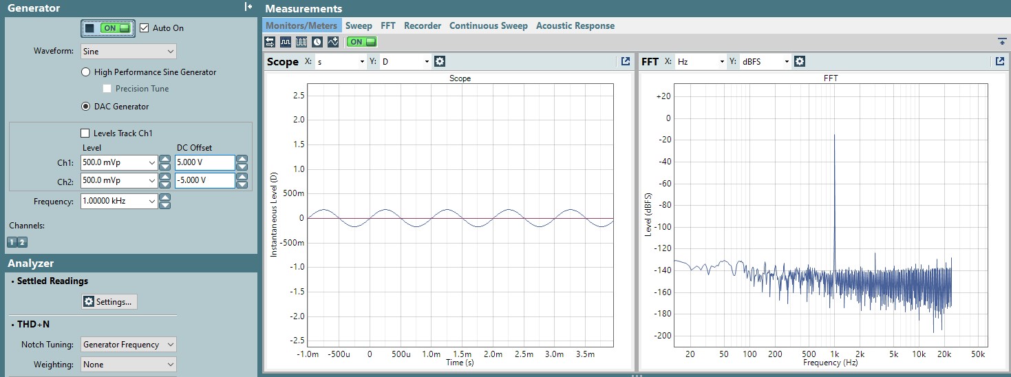 Figure 3-4 0.5-V Pk Signal on DC Bias of
2.5-V-Input Pin Waveform and Digital Capture
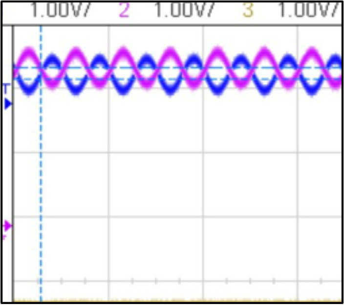 Figure 3-5 Input Pin Waveform 0.5-V Pk
Signal on DC Bias of 2.5 V
Figure 3-5 Input Pin Waveform 0.5-V Pk
Signal on DC Bias of 2.5 VCase 2: When InxP and InxM have a different static DC voltage.
INxP minus INx0 is not equal to zero. There is a DC offset. The internal Digital High Pass Filter can be used to remove this DC offset. If the DC Levels on the pins are close to AVDD or ground, there is reduced headroom for AC signals. The protection diode turns on if the voltage on the input pin exceeds AVDD or is less than ground.
If given a PGA gain, the static DC level at the input also gets a gain. Setting too high a PGA gain leads to the output of the PGA saturating.
Figure 3-6 illustrates an example of pin waveforms on INxP and INxM with different static DC levels.
Let INxP = 2.25 V and INxM = 0.75 V be the static DC levels on the input pins.
Figure 3-6 shows the waveforms on the input pins. Make sure that the pin levels do not exceed 3.3 V or go below 0 V.
Figure 3-6 also shows the difference (INxP – INxM). There is a DC offset of 1.5 V which is seen in ADC output. The digital high pass filter removes this offset.
 Figure 3-6 Input Pin Waveforms With
Different Static DC Levels
Figure 3-6 Input Pin Waveforms With
Different Static DC LevelsFigure 3-7 shows a 1-Vrms signal with a DC offset of 1.5 V. A larger signal can result in harmonics appearing on the FFT.
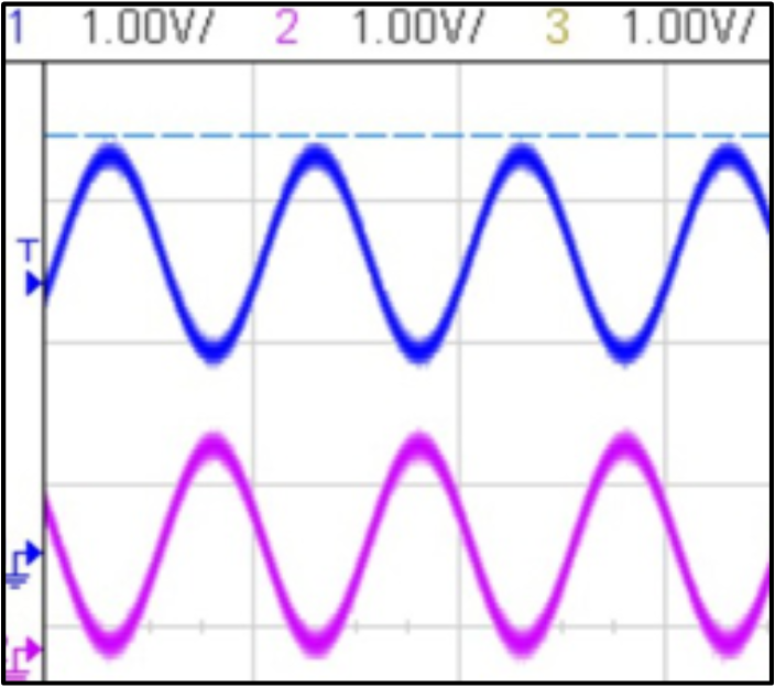 Figure 3-7 Waveforms at INxP and INxM
Pins
Figure 3-7 Waveforms at INxP and INxM
PinsThe DC offset between the two input pins can be seen at the digital output capture if HPF_SEL has 00b which enables an all pass filter.
If HPF_SEL is set for high-pass filter, this DC component is removed in the digital output capture.
| Bit | Field | Type | Reset | Description |
|---|---|---|---|---|
| 1-0 | HPF_SEL[1:0] | R/W | 1h | High-pass filter
(HPF) selection. 0d = Programmable first-order IIR filter for a custom HPF with default coefficient values in P4_R72 to P4_R83 set as the all-pass filter 1d = HPF with a cutoff of 0.00025 × fS (12 Hz at fS = 48 kHz) is selected 2d = HPF with a cutoff of 0.002 × fS (96 Hz at fS = 48 kHz) is selected 3d = HPF with a cutoff of 0.008 × fS (384 Hz at fS = 48 kHz) is selected |
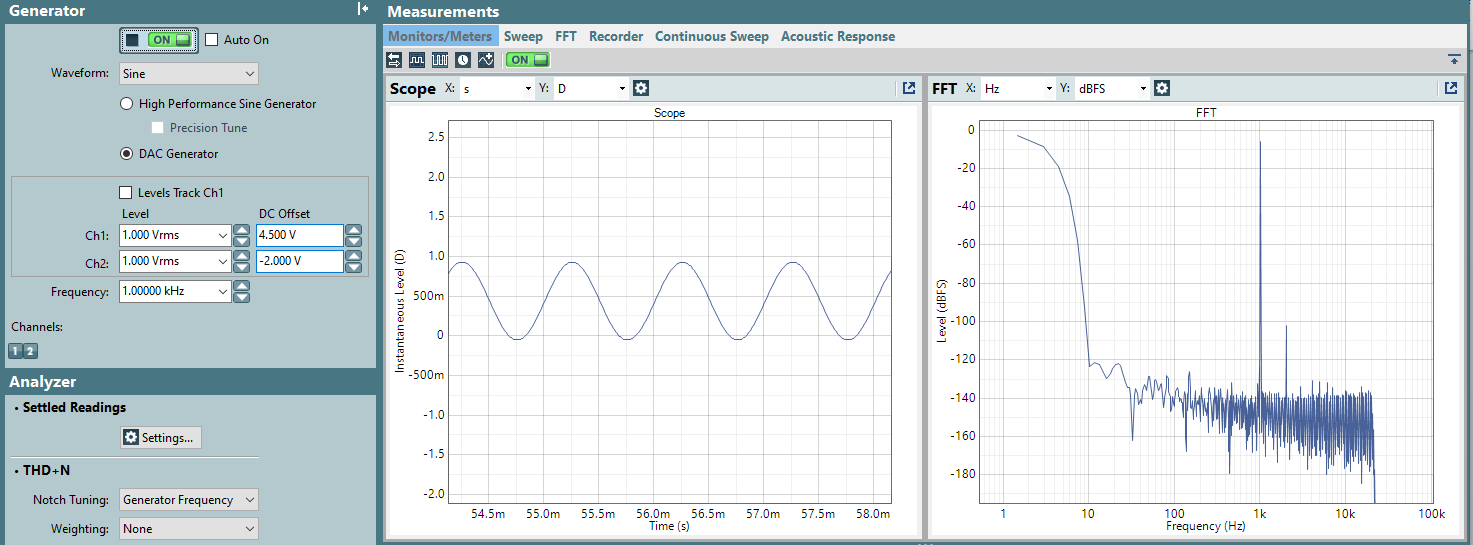 Figure 3-8 Digital Capture With All Pass
Filter - DC Offset is Seen
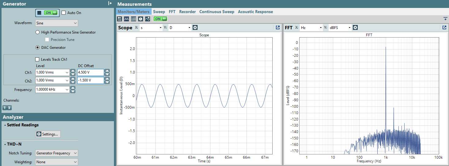 Figure 3-9 Digital Capture With Low-Pass
Filter