SBAU382A November   2021  – January 2022 ADS7029-Q1 , ADS7039-Q1 , ADS7040 , ADS7041 , ADS7042 , ADS7043 , ADS7044 , ADS7046 , ADS7047 , ADS7049-Q1 , ADS7052 , ADS7054 , ADS7056 , ADS7057


  1.   Trademarks
  2. 1ADS704X-5XEVM-PDK Overview
  3. 2Introduction to the ADS704X-5XEVM
    1. 2.1 Analog Inputs
      1. 2.1.1 Single-Ended Input Path
      2. 2.1.2 Differential Input Path
    2. 2.2 Power Supplies
    3. 2.3 Digital Interface and Communication
    4. 2.4 I2C Bus for Onboard EEPROM
  4. 3ADS704X-5XEVM Software Installation
  5. 4EVM Operation
    1. 4.1 Connecting the Hardware
    2. 4.2 EVM GUI Global Settings for ADC Control
    3. 4.3 Time Domain Display
    4. 4.4 Spectral Analysis
    5. 4.5 Histogram Analysis
    6. 4.6 Updating EEPROM After ADC Replacement
  6. 5Bill of Materials, Layout, and Schematic
    1. 5.1 Bill of Materials
    2. 5.2 Layout
    3. 5.3 Schematic
  7. 6Revision History

Layout

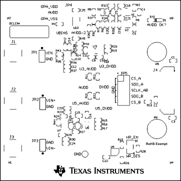
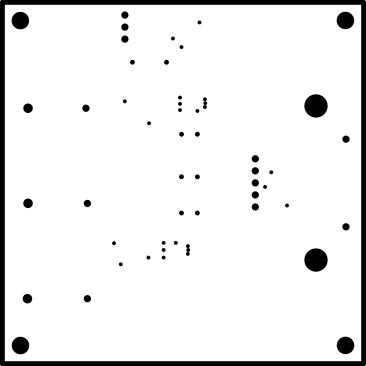
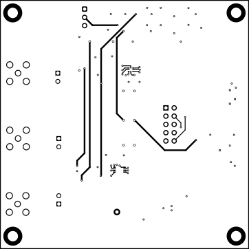
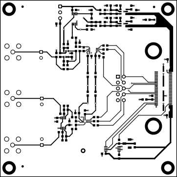
Figure 5-1 through Figure 5-7 show the layout for the ADS704X-5XEVM.
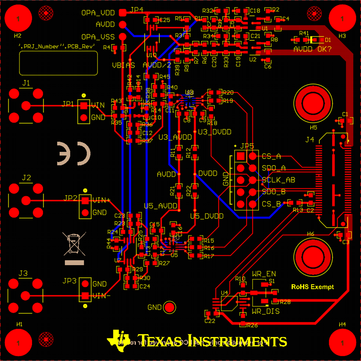
GUID-20211028-SS0I-MBHR-WKKD-NZ4S9FJRGHSW-low.png Figure 5-1 Composite PCB Layout
GUID-20211018-SS0I-RXTH-W1G5-FSBLWDKSR23S-low.gifFigure 5-2 Top Overlay
GUID-20211018-SS0I-8G2P-GRB3-F75L6KBDCTRG-low.gifFigure 5-4 Inner Ground Plane 1
GUID-20211018-SS0I-BLNF-5V1V-TRFGCDXZFPZZ-low.gifFigure 5-6 Bottom Layer
GUID-20211018-SS0I-CF4T-ZCBQ-F5PS1GHF3BDP-low.gifFigure 5-3 Top Layer
GUID-20211018-SS0I-8G2P-GRB3-F75L6KBDCTRG-low.gifFigure 5-5 Inner Ground Plane 2
GUID-20211018-SS0I-Q5KV-MR81-53G5FCXGNZJJ-low.gifFigure 5-7 Bottom Overlay